P r e l i m i n a ry D a t a S h e et , D S 1 , N o v . 2 00 1
SWITI
Switching IC
PEF 20450
MTSI
PEF 20470
MTSI-L
PEF 24470
MTSI-XL
V er s i o n 1 . 3
Wi r ed
Communications
N e v e r
s t o p
t h i n k i n g .
�Edition 2001-11-20
Published by Infineon Technologies AG,
St.-Martin-Strasse 53,
D-81541 München, Germany
© Infineon Technologies AG 2001.
All Rights Reserved.
Attention please!
The information herein is given to describe certain components and shall not be considered as warranted
characteristics.
Terms of delivery and rights to technical change reserved.
We hereby disclaim any and all warranties, including but not limited to warranties of non-infringement, regarding
circuits, descriptions and charts stated herein.
Infineon Technologies is an approved CECC manufacturer.
Information
For further information on technology, delivery terms and conditions and prices please contact your nearest
Infineon Technologies Office in Germany or our Infineon Technologies Representatives worldwide (see address
list).
Warnings
Due to technical requirements components may contain dangerous substances. For information on the types in
question please contact your nearest Infineon Technologies Office.
Infineon Technologies Components may only be used in life-support devices or systems with the express written
approval of Infineon Technologies, if a failure of such components can reasonably be expected to cause the failure
of that life-support device or system, or to affect the safety or effectiveness of that device or system. Life support
devices or systems are intended to be implanted in the human body, or to support and/or maintain and sustain
and/or protect human life. If they fail, it is reasonable to assume that the health of the user or other persons may
be endangered.
�Y
P r e l i m i n a ry D a t a S h e et , D S 1 , N o v . 2 00 1
PEF 20450
MTSI
MTSI-L
M
PEF 20470
PEF 24470
A
IN
Switching IC
R
SWITI
MTSI-XL
P
R
E
LI
V er s i o n 1 . 3
Wi r ed
Communications
N e v e r
s t o p
t h i n k i n g .
�PEF 20450 / 20470 / 24470
PRELIMINARY
Revision History:
2001-11-20
DS 1
Previous Version:
PEF 20450 / 20470 / 24470 V1.2, Preliminary Data Sheet DS1, 2001-04-04
Page
Content
12
Table 5 updated
26
Chapter 3.4.3 updated, added Figure 9
28
Chapter 3.7.1 and Chapter 3.7.2 updated
30
Chapter 4.2 reworked
49
Description of Configuration Command Register 1 and 2 (CMD1 and
CMD2) updated
57
Description of Interrupt Status Register 1 (ISTA1) reworked
58
Description of Interrupt Error Status Register 1 and 2 (IESTA1 and
IESTA2) reworked
60
Description of Interrupt Error Mask Register 1 and 2 (INTEM1 and INTEM2)
reworked
74
Chapter 6.2 reworked
82
Figure 18 updated
85
Chapter 6.7.3 reworked
101
Chapter 7.1 and Table 22 updated
104
Table 23 updated
110
Table 27 and Figure 39 updated
112
Added Chapter, 7.5“Hardware Reset Timing”
115
Table 32 updated.
For questions on technology, delivery and prices please contact the Infineon
Technologies Offices in Germany or the Infineon Technologies Companies and
Representatives worldwide: see our webpage at http://www.infineon.com
�PEF 20450 / 20470 / 24470
Table of Contents
Page
1
1.1
1.2
1.3
1.4
Overview . . . . . . . . . . . . . . . . . . . . . . . . . . . . . . . . . . . . . . . . . . . . . . . . . . . 3
Overview of Features . . . . . . . . . . . . . . . . . . . . . . . . . . . . . . . . . . . . . . . . . . 5
Features in Detail . . . . . . . . . . . . . . . . . . . . . . . . . . . . . . . . . . . . . . . . . . . . . 6
Logic Symbol . . . . . . . . . . . . . . . . . . . . . . . . . . . . . . . . . . . . . . . . . . . . . . . . 8
Standard PBX or CO Application . . . . . . . . . . . . . . . . . . . . . . . . . . . . . . . . 10
2
2.1
2.2
2.2.1
2.2.2
2.2.3
2.2.4
2.2.5
2.2.6
Pin Description . . . . . . . . . . . . . . . . . . . . . . . . . . . . . . . . . . . . . . . . . . . .
Pin Diagrams . . . . . . . . . . . . . . . . . . . . . . . . . . . . . . . . . . . . . . . . . . . . . . .
Pin Definitions and Functions . . . . . . . . . . . . . . . . . . . . . . . . . . . . . . . . . .
Local Bus Interface (PCM) . . . . . . . . . . . . . . . . . . . . . . . . . . . . . . . . . . .
General Purpose Port . . . . . . . . . . . . . . . . . . . . . . . . . . . . . . . . . . . . . .
Clock Signals . . . . . . . . . . . . . . . . . . . . . . . . . . . . . . . . . . . . . . . . . . . . .
JTAG Interface . . . . . . . . . . . . . . . . . . . . . . . . . . . . . . . . . . . . . . . . . . . .
Microprocessor Interface . . . . . . . . . . . . . . . . . . . . . . . . . . . . . . . . . . . .
Power Supply . . . . . . . . . . . . . . . . . . . . . . . . . . . . . . . . . . . . . . . . . . . . .
11
11
12
12
12
12
13
13
14
3
3.1
3.2
3.3
3.3.1
3.3.1.1
3.3.1.2
3.3.1.3
3.3.1.4
3.3.1.5
3.3.1.6
3.3.2
3.3.3
3.3.4
3.4
3.4.1
3.4.2
3.4.2.1
3.4.2.2
3.4.3
3.4.4
3.5
3.6
3.7
3.7.1
3.7.2
Architectural Description . . . . . . . . . . . . . . . . . . . . . . . . . . . . . . . . . . . .
Functional Block Diagram . . . . . . . . . . . . . . . . . . . . . . . . . . . . . . . . . . . . .
Overview of Functional Blocks . . . . . . . . . . . . . . . . . . . . . . . . . . . . . . . . . .
Switching Factory . . . . . . . . . . . . . . . . . . . . . . . . . . . . . . . . . . . . . . . . . . .
Switching Modes . . . . . . . . . . . . . . . . . . . . . . . . . . . . . . . . . . . . . . . . . .
Minimum and Constant Delay . . . . . . . . . . . . . . . . . . . . . . . . . . . . . .
Subchannel Switching . . . . . . . . . . . . . . . . . . . . . . . . . . . . . . . . . . . .
Multipoint Switching . . . . . . . . . . . . . . . . . . . . . . . . . . . . . . . . . . . . . .
Broadcast Switching . . . . . . . . . . . . . . . . . . . . . . . . . . . . . . . . . . . . .
Bidirectional Switching . . . . . . . . . . . . . . . . . . . . . . . . . . . . . . . . . . . .
Message Mode . . . . . . . . . . . . . . . . . . . . . . . . . . . . . . . . . . . . . . . . .
Parallel Mode for Local Bus . . . . . . . . . . . . . . . . . . . . . . . . . . . . . . . . . .
Switching Block Error Handling . . . . . . . . . . . . . . . . . . . . . . . . . . . . . . .
Analyze Connection and Data Memory . . . . . . . . . . . . . . . . . . . . . . . . .
Clock Generator and PLL . . . . . . . . . . . . . . . . . . . . . . . . . . . . . . . . . . . . .
General Overview . . . . . . . . . . . . . . . . . . . . . . . . . . . . . . . . . . . . . . . . .
Analog PLL (APLL) . . . . . . . . . . . . . . . . . . . . . . . . . . . . . . . . . . . . . . . .
Functional Description . . . . . . . . . . . . . . . . . . . . . . . . . . . . . . . . . . . .
Jitter Transfer Function . . . . . . . . . . . . . . . . . . . . . . . . . . . . . . . . . . .
Phase Alignment . . . . . . . . . . . . . . . . . . . . . . . . . . . . . . . . . . . . . . . . . .
PLL Synchronization . . . . . . . . . . . . . . . . . . . . . . . . . . . . . . . . . . . . . . .
Loops . . . . . . . . . . . . . . . . . . . . . . . . . . . . . . . . . . . . . . . . . . . . . . . . . . . . .
Read SWITI Configuration with Indirect Register Addressing . . . . . . . . . .
Power-On and Reset Behavior . . . . . . . . . . . . . . . . . . . . . . . . . . . . . . . . .
Hardware Reset . . . . . . . . . . . . . . . . . . . . . . . . . . . . . . . . . . . . . . . . . . .
Software Reset . . . . . . . . . . . . . . . . . . . . . . . . . . . . . . . . . . . . . . . . . . .
15
15
16
17
17
17
17
17
18
18
19
19
20
20
21
21
22
23
25
26
27
27
27
28
28
28
4
Description of Interfaces . . . . . . . . . . . . . . . . . . . . . . . . . . . . . . . . . . . . . 29
Preliminary Data Sheet
2001-11-20
�PEF 20450 / 20470 / 24470
Table of Contents
Page
4.1
4.2
4.3
4.3.1
4.3.2
4.4
4.5
4.5.1
4.5.2
4.6
4.6.1
4.6.2
4.6.3
4.7
Local Bus Interface (PCM) . . . . . . . . . . . . . . . . . . . . . . . . . . . . . . . . . . . . .
Data Rate . . . . . . . . . . . . . . . . . . . . . . . . . . . . . . . . . . . . . . . . . . . . . . . . . .
Microprocessor Interface . . . . . . . . . . . . . . . . . . . . . . . . . . . . . . . . . . . . . .
Intel/Siemens or Motorola Mode . . . . . . . . . . . . . . . . . . . . . . . . . . . . . .
De-multiplexed or Multiplexed Mode . . . . . . . . . . . . . . . . . . . . . . . . . . .
General Purpose Port (GPIO) . . . . . . . . . . . . . . . . . . . . . . . . . . . . . . . . . .
General Purpose Clocks . . . . . . . . . . . . . . . . . . . . . . . . . . . . . . . . . . . . . .
Frame Group Outputs . . . . . . . . . . . . . . . . . . . . . . . . . . . . . . . . . . . . . .
GPCLK as Clock Outputs . . . . . . . . . . . . . . . . . . . . . . . . . . . . . . . . . . .
JTAG (Boundary Scan) . . . . . . . . . . . . . . . . . . . . . . . . . . . . . . . . . . . . . . .
Boundary Scan . . . . . . . . . . . . . . . . . . . . . . . . . . . . . . . . . . . . . . . . . . .
Test-Access-Port (TAP) . . . . . . . . . . . . . . . . . . . . . . . . . . . . . . . . . . . . .
TAP Controller . . . . . . . . . . . . . . . . . . . . . . . . . . . . . . . . . . . . . . . . . . . .
Identification Code via µP Read Access . . . . . . . . . . . . . . . . . . . . . . . . . .
29
30
31
31
31
33
33
34
34
35
35
35
36
38
5
5.1
5.2
5.3
5.4
Register Description . . . . . . . . . . . . . . . . . . . . . . . . . . . . . . . . . . . . . . . .
Register Overview For 8-Bit Interface . . . . . . . . . . . . . . . . . . . . . . . . . . . .
Detailed Register Description For 8-bit Interface . . . . . . . . . . . . . . . . . . . .
Register Overview For 16-Bit Interface . . . . . . . . . . . . . . . . . . . . . . . . . . .
Detailed Register Description For 16-Bit Interface . . . . . . . . . . . . . . . . . .
39
40
42
67
68
6
6.1
6.2
6.3
6.4
6.5
6.6
6.7
6.7.1
6.7.2
6.7.3
6.7.3.1
6.7.3.2
6.8
6.8.1
6.9
6.10
6.10.1
6.10.2
6.10.2.1
6.10.2.2
6.10.2.3
6.10.3
Programming the Device . . . . . . . . . . . . . . . . . . . . . . . . . . . . . . . . . . . .
Read and Write Access . . . . . . . . . . . . . . . . . . . . . . . . . . . . . . . . . . . . . . .
Interrupt Handling . . . . . . . . . . . . . . . . . . . . . . . . . . . . . . . . . . . . . . . . . . .
Command and Register Overview . . . . . . . . . . . . . . . . . . . . . . . . . . . . . . .
Indirect Configuration Register Access . . . . . . . . . . . . . . . . . . . . . . . . . . .
Initialization Procedure . . . . . . . . . . . . . . . . . . . . . . . . . . . . . . . . . . . . . . .
Clocking Unit . . . . . . . . . . . . . . . . . . . . . . . . . . . . . . . . . . . . . . . . . . . . . . .
Local Bus (PCM) Line Interface . . . . . . . . . . . . . . . . . . . . . . . . . . . . . . . . .
Standby Command . . . . . . . . . . . . . . . . . . . . . . . . . . . . . . . . . . . . . . . .
Determining Clock Rates . . . . . . . . . . . . . . . . . . . . . . . . . . . . . . . . . . . .
Performing Bit Shifting . . . . . . . . . . . . . . . . . . . . . . . . . . . . . . . . . . . . . .
Input Bit Shifting . . . . . . . . . . . . . . . . . . . . . . . . . . . . . . . . . . . . . . . . .
Output Bit Shifting . . . . . . . . . . . . . . . . . . . . . . . . . . . . . . . . . . . . . . .
Global Clock Signals . . . . . . . . . . . . . . . . . . . . . . . . . . . . . . . . . . . . . . . . .
Framing Groups . . . . . . . . . . . . . . . . . . . . . . . . . . . . . . . . . . . . . . . . . . .
Read Time-Slot Value . . . . . . . . . . . . . . . . . . . . . . . . . . . . . . . . . . . . . . . .
Establish Connections . . . . . . . . . . . . . . . . . . . . . . . . . . . . . . . . . . . . . . . .
Establish 8-bit Connections . . . . . . . . . . . . . . . . . . . . . . . . . . . . . . . . . .
Subchannel Switching . . . . . . . . . . . . . . . . . . . . . . . . . . . . . . . . . . . . . .
Establish 4-bit Connections . . . . . . . . . . . . . . . . . . . . . . . . . . . . . . . .
Establish 2-bit Connections . . . . . . . . . . . . . . . . . . . . . . . . . . . . . . . .
Establish 1-bit Connections . . . . . . . . . . . . . . . . . . . . . . . . . . . . . . . .
Establish Broadcast Connections . . . . . . . . . . . . . . . . . . . . . . . . . . . . .
72
73
74
76
81
82
83
84
84
84
85
85
86
87
87
88
89
89
90
90
91
92
93
Preliminary Data Sheet
2001-11-20
�PEF 20450 / 20470 / 24470
Table of Contents
Page
6.10.4
6.10.5
6.11
6.12
6.12.1
6.12.2
6.12.3
6.12.4
6.12.5
6.12.6
6.12.7
6.13
Establish Subchannel Broadcast Connection . . . . . . . . . . . . . . . . . . . . 94
Establish Multipoint Connection . . . . . . . . . . . . . . . . . . . . . . . . . . . . . . . 95
Send Messages . . . . . . . . . . . . . . . . . . . . . . . . . . . . . . . . . . . . . . . . . . . . . 96
Release Connections . . . . . . . . . . . . . . . . . . . . . . . . . . . . . . . . . . . . . . . . . 97
Release 8-bit Connections . . . . . . . . . . . . . . . . . . . . . . . . . . . . . . . . . . . 97
Release 4-bit Connections . . . . . . . . . . . . . . . . . . . . . . . . . . . . . . . . . . . 97
Release 2-bit Connections . . . . . . . . . . . . . . . . . . . . . . . . . . . . . . . . . . . 97
Release 1-bit Connections . . . . . . . . . . . . . . . . . . . . . . . . . . . . . . . . . . . 98
Release Broadcast Connection . . . . . . . . . . . . . . . . . . . . . . . . . . . . . . . 99
Release Subchannel Broadcast Connection . . . . . . . . . . . . . . . . . . . . . 99
Release Multipoint Connection . . . . . . . . . . . . . . . . . . . . . . . . . . . . . . 100
Stop Sending Messages . . . . . . . . . . . . . . . . . . . . . . . . . . . . . . . . . . . . . 100
7
7.1
7.2
7.3
7.3.1
7.3.2
7.3.3
7.4
7.5
Timing Diagrams . . . . . . . . . . . . . . . . . . . . . . . . . . . . . . . . . . . . . . . . . .
PCM Interface Timing . . . . . . . . . . . . . . . . . . . . . . . . . . . . . . . . . . . . . . .
PCM Parallel Mode Timing . . . . . . . . . . . . . . . . . . . . . . . . . . . . . . . . . . .
Microprocessor Interface Timing . . . . . . . . . . . . . . . . . . . . . . . . . . . . . . .
Infineon/Intel Timing in De-Multiplexed Mode . . . . . . . . . . . . . . . . . . .
Infineon/Intel Timing in Multiplexed Mode . . . . . . . . . . . . . . . . . . . . . .
Motorola Microprocessor Timing . . . . . . . . . . . . . . . . . . . . . . . . . . . . .
JTAG Interface Timing . . . . . . . . . . . . . . . . . . . . . . . . . . . . . . . . . . . . . . .
Hardware Reset Timing . . . . . . . . . . . . . . . . . . . . . . . . . . . . . . . . . . . . . .
101
101
104
105
105
106
108
110
112
8
8.1
8.2
8.3
8.4
8.5
8.6
Electrical Characteristics . . . . . . . . . . . . . . . . . . . . . . . . . . . . . . . . . . .
Absolute Maximum Ratings . . . . . . . . . . . . . . . . . . . . . . . . . . . . . . . . . . .
Operating Range . . . . . . . . . . . . . . . . . . . . . . . . . . . . . . . . . . . . . . . . . . .
Crystal Oscillator . . . . . . . . . . . . . . . . . . . . . . . . . . . . . . . . . . . . . . . . . . .
DC Characteristics . . . . . . . . . . . . . . . . . . . . . . . . . . . . . . . . . . . . . . . . . .
Capacitances . . . . . . . . . . . . . . . . . . . . . . . . . . . . . . . . . . . . . . . . . . . . . .
AC Characteristics . . . . . . . . . . . . . . . . . . . . . . . . . . . . . . . . . . . . . . . . . .
113
113
113
114
115
115
116
9
Package Outlines . . . . . . . . . . . . . . . . . . . . . . . . . . . . . . . . . . . . . . . . . . 117
Preliminary Data Sheet
2001-11-20
�PEF 20450 / 20470 / 24470
List of Figures
Figure 1
Figure 2
Figure 3
Figure 4
Figure 5
Figure 6
Figure 7
Figure 8
Figure 9
Figure 10
Figure 11
Figure 12
Figure 13
Figure 14
Figure 15
Figure 16
Figure 17
Figure 18
Figure 19
Figure 20
Figure 21
Figure 22
Figure 23
Figure 24
Figure 25
Figure 26
Figure 27
Figure 28
Figure 29
Figure 30
Figure 31
Figure 32
Figure 33
Figure 34
Figure 35
Figure 36
Figure 37
Figure 38
Figure 39
Figure 40
Figure 41
Figure 42
Figure 43
Page
Logic Symbol . . . . . . . . . . . . . . . . . . . . . . . . . . . . . . . . . . . . . . . . . . . . . 9
Standard PBX or CO Application . . . . . . . . . . . . . . . . . . . . . . . . . . . . . 10
Pin Configuration . . . . . . . . . . . . . . . . . . . . . . . . . . . . . . . . . . . . . . . . . 11
Block Diagram . . . . . . . . . . . . . . . . . . . . . . . . . . . . . . . . . . . . . . . . . . . 15
Bidirectional Mode . . . . . . . . . . . . . . . . . . . . . . . . . . . . . . . . . . . . . . . . 19
SWITI Clock Generator . . . . . . . . . . . . . . . . . . . . . . . . . . . . . . . . . . . . 21
Block Diagram of APLL . . . . . . . . . . . . . . . . . . . . . . . . . . . . . . . . . . . . 23
APLL - Jitter Transfer Function . . . . . . . . . . . . . . . . . . . . . . . . . . . . . . 25
Example of Phase Alignment . . . . . . . . . . . . . . . . . . . . . . . . . . . . . . . . 26
PCM Interface Configurations . . . . . . . . . . . . . . . . . . . . . . . . . . . . . . . 29
PCM Bit Shifting . . . . . . . . . . . . . . . . . . . . . . . . . . . . . . . . . . . . . . . . . . 30
Multiplexed and in De-multiplexed Bus Mode . . . . . . . . . . . . . . . . . . . 32
GPIO Port Configuration Example . . . . . . . . . . . . . . . . . . . . . . . . . . . . 33
Frame Signal Example. . . . . . . . . . . . . . . . . . . . . . . . . . . . . . . . . . . . . 34
Order of Register Access. . . . . . . . . . . . . . . . . . . . . . . . . . . . . . . . . . . 72
8-bit µP Access Interrupt Structure . . . . . . . . . . . . . . . . . . . . . . . . . . . 74
16-bit µP Access Interrupt Structure . . . . . . . . . . . . . . . . . . . . . . . . . . 75
Initialization Procedure after Reset . . . . . . . . . . . . . . . . . . . . . . . . . . . 82
Example: Input Bit Shifting . . . . . . . . . . . . . . . . . . . . . . . . . . . . . . . . . . 85
Example: Output Bit Shifting . . . . . . . . . . . . . . . . . . . . . . . . . . . . . . . . 86
Example Framing Groups . . . . . . . . . . . . . . . . . . . . . . . . . . . . . . . . . . 87
Example: 8-bit Connection . . . . . . . . . . . . . . . . . . . . . . . . . . . . . . . . . . 89
Subchannel Address in Time-Slot . . . . . . . . . . . . . . . . . . . . . . . . . . . . 90
Example: 4-bit Connection . . . . . . . . . . . . . . . . . . . . . . . . . . . . . . . . . . 90
Example: 2-bit Connection . . . . . . . . . . . . . . . . . . . . . . . . . . . . . . . . . . 91
Example: 1-bit Connection . . . . . . . . . . . . . . . . . . . . . . . . . . . . . . . . . . 92
Example: Broadcast Connection . . . . . . . . . . . . . . . . . . . . . . . . . . . . . 93
Example: Subchannel Broadcast Connection . . . . . . . . . . . . . . . . . . . 94
Example: Multipoint Connection . . . . . . . . . . . . . . . . . . . . . . . . . . . . . 95
Example: Send Message . . . . . . . . . . . . . . . . . . . . . . . . . . . . . . . . . . . 96
PCM Timing . . . . . . . . . . . . . . . . . . . . . . . . . . . . . . . . . . . . . . . . . . . . 101
Parallel Mode Timing . . . . . . . . . . . . . . . . . . . . . . . . . . . . . . . . . . . . . 104
Infineon/Intel Read Cycle in De-Multiplexed Mode . . . . . . . . . . . . . . 106
Infineon/Intel Write Cycle in De-Multiplexed Mode . . . . . . . . . . . . . . 106
Infineon/Intel Read Cycle in Multiplexed Mode . . . . . . . . . . . . . . . . . 107
Infineon/Intel Write Cycle in Multiplexed Mode . . . . . . . . . . . . . . . . . 108
Motorola Read Cycle . . . . . . . . . . . . . . . . . . . . . . . . . . . . . . . . . . . . . 109
Motorola Write Cycle . . . . . . . . . . . . . . . . . . . . . . . . . . . . . . . . . . . . . 109
Boundary Scan Timing. . . . . . . . . . . . . . . . . . . . . . . . . . . . . . . . . . . . 111
Hardware Reset Timing . . . . . . . . . . . . . . . . . . . . . . . . . . . . . . . . . . . 112
External Crystal . . . . . . . . . . . . . . . . . . . . . . . . . . . . . . . . . . . . . . . . . 114
I/O Wave Form for AC-Test . . . . . . . . . . . . . . . . . . . . . . . . . . . . . . . . 116
Outlines of P-MQFP-100-2 . . . . . . . . . . . . . . . . . . . . . . . . . . . . . . . . 117
Preliminary Data Sheet
2001-11-20
�PEF 20450 / 20470 / 24470
List of Table
Table 1
Table 2
Table 3
Table 4
Table 5
Table 6
Table 7
Table 8
Table 9
Table 10
Table 11
Table 12
Table 13
Table 14
Table 15
Table 16
Table 17
Table 18
Table 19
Table 20
Table 21
Table 22
Table 23
Table 24
Table 25
Table 26
Table 27
Table 28
Table 29
Table 30
Table 31
Table 32
Table 33
Page
Who should read what? . . . . . . . . . . . . . . . . . . . . . . . . . . . . . . . . . . . . . 2
SWITI Family Tree . . . . . . . . . . . . . . . . . . . . . . . . . . . . . . . . . . . . . . . . . 3
Local Bus Interface . . . . . . . . . . . . . . . . . . . . . . . . . . . . . . . . . . . . . . . 12
GPIO . . . . . . . . . . . . . . . . . . . . . . . . . . . . . . . . . . . . . . . . . . . . . . . . . . 12
Clock Pins . . . . . . . . . . . . . . . . . . . . . . . . . . . . . . . . . . . . . . . . . . . . . . 12
JTAG Interface . . . . . . . . . . . . . . . . . . . . . . . . . . . . . . . . . . . . . . . . . . . 13
Microprocessor Interface . . . . . . . . . . . . . . . . . . . . . . . . . . . . . . . . . . . 13
Power Supply Pins . . . . . . . . . . . . . . . . . . . . . . . . . . . . . . . . . . . . . . . . 14
TAP Controller Instructions . . . . . . . . . . . . . . . . . . . . . . . . . . . . . . . . . 36
Boundary Scan IDCODE . . . . . . . . . . . . . . . . . . . . . . . . . . . . . . . . . . . 37
IDCODE via µP Read Access . . . . . . . . . . . . . . . . . . . . . . . . . . . . . . . 38
Register Overview For 8-Bit Interface . . . . . . . . . . . . . . . . . . . . . . . . . 40
Value Range for SPA/DPA . . . . . . . . . . . . . . . . . . . . . . . . . . . . . . . . . 41
Value Range for ITSA/OTSA . . . . . . . . . . . . . . . . . . . . . . . . . . . . . . . . 41
Value Range for SCA. . . . . . . . . . . . . . . . . . . . . . . . . . . . . . . . . . . . . . 41
Register Overview For 16-Bit Interface . . . . . . . . . . . . . . . . . . . . . . . . 67
Affected Registers for Connection Commands . . . . . . . . . . . . . . . . . . 76
Affected Registers for Configuration Commands. . . . . . . . . . . . . . . . . 77
Connection Command and Parameter Codes . . . . . . . . . . . . . . . . . . . 78
Configuration Command 1 and Parameter Codes . . . . . . . . . . . . . . . . 79
Configuration Command 2 and Parameter Code. . . . . . . . . . . . . . . . . 79
PCM Timing . . . . . . . . . . . . . . . . . . . . . . . . . . . . . . . . . . . . . . . . . . . . 102
PCM Parallel Mode Timing . . . . . . . . . . . . . . . . . . . . . . . . . . . . . . . . 104
Infineon/Intel Timing in De-Multiplexed Mode . . . . . . . . . . . . . . . . . . 105
Infineon/Intel Timing in Multiplexed Mode . . . . . . . . . . . . . . . . . . . . . 107
Motorola Timing . . . . . . . . . . . . . . . . . . . . . . . . . . . . . . . . . . . . . . . . . 108
JTAG Interface Timing . . . . . . . . . . . . . . . . . . . . . . . . . . . . . . . . . . . . 110
Hardware Reset Timing . . . . . . . . . . . . . . . . . . . . . . . . . . . . . . . . . . . 112
Absolute Maximum Ratings . . . . . . . . . . . . . . . . . . . . . . . . . . . . . . . . 113
Operating Range . . . . . . . . . . . . . . . . . . . . . . . . . . . . . . . . . . . . . . . . 113
External Capacitances for Crystal (Recommendation) . . . . . . . . . . . 114
DC Characteristics . . . . . . . . . . . . . . . . . . . . . . . . . . . . . . . . . . . . . . . 115
Input/Output Capacitances . . . . . . . . . . . . . . . . . . . . . . . . . . . . . . . . 115
Preliminary Data Sheet
2001-11-20
�PEF 20450 / 20470 / 24470
PRELIMINARY
Preface
The Switching IC (SWITI) is a family of switching devices for a wide area of
telecommunication and data communication applications. This document provides
complete reference information according to chip interfaces, programming, internal
architecture and applications.
Organization of this Document
This Preliminary Data Sheet is divided into 9 chapters. It is organized as follows:
• Chapter 1, Overview
Gives a general description of the product and its family, lists the key features, and
presents some typical applications.
• Chapter 2, Pin Description
Lists pin locations with associated signals, categorizes signals according to function,
and describes signals.
• Chapter 3, Description of Interfaces
Rough overview of the internal architecture.
• Chapter 4, Description of Interfaces
Short introduction of used interfaces.
• Chapter 5, Register Description
Gives information about all registers accessible via the microprocessor interface
according to address, short name, access, reset value and value range.
• Chapter 6, Programming the Device
Gives a variety of examples how to programm the device, lists all available command
and parameter values.
• Chapter 7, Timing Diagrams
Contains timing diagrams.
• Chapter 8, Electrical Characteristics
Specification of the electrical parameters.
• Chapter 9, Package Outlines
Outlines of the available packages (P-MQFP-100-2).
Preliminary Data Sheet
1
2001-11-20
�PEF 20450 / 20470 / 24470
PRELIMINARY
Table 1
Who should read what?
Addressed Person
Relevant Chapters
Programmer
3, 5, 6
Board Designer
2, 3, 4, 7, 8, 9
Preliminary Data Sheet
2
2001-11-20
�PEF 20450 / 20470 / 24470
Overview
PRELIMINARY
1
Overview
The new switching family, called SWITI, provides a complete and cost-effective solution
for all switching systems. The family is divided in two sub-families, the MTSI family and
the HTSI family. The Preliminary Data Sheet describes the functionality and
characteristic of the MTSI devices.
The devices can be used in today’s switching applications, e.g. conventional PBXs and
central offices, as well as in H.100/H.110 applications (only the HTSI family), which are
the key to high performing CTI- and Voice-over-IP-applications, one of the most
important future technologies in telecommunications.
The main requirements of today’s switching applications are met by the following
features:
• Constant delay e.g. to support wide band data switching, or channel bundling
• Bit switching/subchannel switching to support applications such as mobile base
stations, DECT, computer telephony
In addition, the SWITI family provides new features to ensure a broad range of
configurations to make it possible to adapt the device to all switching applications:
•
•
•
•
A compliant H.100/H.110 interface (HTSI)
8-channel stream-to-stream switching capability (HTSI)
Message mode, which allows to assign a preset value to any output time-slot
GPIO (General Purpose I/O) port, which is controlled from the external µP
SWITI family. The SWITI family consists of 6 ICs with different switching capacities. The
possible configurations are shown in Table 2. The HTSI versions provide an additional
H.100 / H.110 interface, while the MTSIs are standard switching devices. All devices can
be programmed easily, thus helping the designer/programmer to integrate the device
into his application comfortably.
Table 2
SWITI Family Tree
Name
HTSI-XL (H-Mode)
Package
P-BGA-217-1
HTSI-XL (M-Mode)
HTSI-L (H-Mode)
HTSI-L (M-Mode)
Preliminary Data Sheet
Sales
code
Connections
Local bus
IN/OUT
H-Bus IO
PEF 24471
HTSI-XL
2048
16/16
32
32/32
-
16/16
32
32/32
-
PEF 24471
HTSI-XL
P-BGA-217-1
PEF 20471
HTSI-L
PEF 20471
HTSI-L
3
1024
2001-11-20
�PEF 20450 / 20470 / 24470
Overview
PRELIMINARY
Table 2
SWITI Family Tree (cont’d)
Name
HTSI (H-Mode)
HTSI (M-Mode)
Package
P-BGA-217-1
Sales
code
Connections
Local bus
IN/OUT
H-Bus IO
PEF 20451
HTSI
512
16/16
32
32/32
-
PEF 20451
HTSI
MTSI-XL
P-MQFP-100-2 PEF 24470
MTSI-XL
2048
16/16
-
MTSI-L
P-MQFP-100-2 PEF 20470
MTSI-L
1024
16/16
-
MTSI
P-MQFP-100-2 PEF 20450
MTSI
512
16/16
-
Preliminary Data Sheet
4
2001-11-20
�PRELIMINARY
Switching IC
SWITI
PEF 20450 / 20470 / 24470
Version 1.3
1.1
CMOS
Overview of Features
General
• Switching capacity of 512, 1024, or up to 2048
connections of different types between different
buses
• Programmable data rates of 2.048 Mbit/s,
P-MQFP-100-2
4.096 Mbit/s, 8.192 Mbit/s, and 16.384 Mbit/s on per
stream basis
• 16 PCM Highways (IN/OUT)
• Constant delay or minimum delay programmable on per connection basis
• Subchannel switching ability of 1-bit, 2-bit, 4-bit wide time-slots
• Programmable clock shift for local bus
• Automatic data rate adaption
• Optional 8-bit parallel input and/or 8-bit parallel output for first 8 lines of local bus
• Broadcast capabilities
• Multipoint switching ability
• Read and write access to all time-slots
• Message mode (time-slot write access)
• Programmable framing group
• GPIO port
• 8-bit µP-interface supports both Intel and Motorola mode
• Optional 16-bit µP interface mode (instead of GPIO port)
• On chip PLL for PCM bus clock operation (master/slave)
• JTAG interface
– Boundary scan according to IEEE 1149.1
• 3.3 V power supply
• 5 V tolerant inputs/outputs
Type
Package
PEF 20450 / 20470 / 24470
P-MQFP-100-2
Preliminary Data Sheet
5
2001-11-20
�PEF 20450 / 20470 / 24470
Overview
PRELIMINARY
1.2
Features in Detail
Flexible Data Rates
Each input and each output line of the local bus is programmable to operate at different
data rates. The possible data rates are 2.048 Mbit/s, 4.096 Mbit/s, 8.192 Mbit/s, and
16.384 Mbit/s.
Constant and Minimum Delay
Each connection independent of the addressed buses can be determined to be a
constant delay or minimum delay connection. Constant delay means that any input timeslot or subchannel is available on the programmed output after 2 frames. Minimum delay
means that the time-slot or subchannel appears at the output as soon as possible. The
minimum delay depends on the chosen connections and the possible range is between
0 and 2 frames.
Subchannel Switching
Each connection can be a 1-bit, 2-bit, 4-bit, or 8-bit connection. Subchannel switching
has a constant delay of 2 frames. Subchannel switching is supported only for data rate
of 2.048 Mbit/s, 4.096 Mbit/s and 8.192 Mbit/s.
Programmable Clock Shift
The position of time-slot 0 of each local bus input line can be programmed within the
time-slot before and after the PFS rising edge in half bit steps. Also the position of timeslot 0 of all local bus output lines can be programmed within the first time-slot after the
PFS rising edge.
Automatic Data Rate Adaption
Connections are also possible between lines operating at different data rates. The
programmer just specifies input and output line, time-slot, and if necessary, the
subchannel.
Parallel Mode
The first 8 local bus input and output lines can be configured to one parallel input or
output port respectively. In serial mode a time-slot is determined by 8 consecutive data
clock cycles according to each line. In parallel mode a time-slot is determined by 1 data
clock cycle according to the first 8 lines.
Preliminary Data Sheet
6
2001-11-20
�PEF 20450 / 20470 / 24470
Overview
PRELIMINARY
Broadcast
With this feature it is possible to distribute one incoming time-slot to different output timeslots.
Multipoint
Multipoint connections can be seen as the opposite of broadcast connections. Here it is
possible to generate one output time-slot consisting of several input time-slots. The
specified input time-slots are logically AND or OR connected (selectable) and have a
constant delay of 2 frames.
Read Access
The programmer has access to any input time-slot. After issuing an appropriate
command the arrival of the time-slot will be reported by interrupt. The value can be read
from a dedicated register. For every read request the command has to be issued again.
Message Mode (Write Access)
This feature allows a constant value to be sent to any given output time-slot.
Framing Group
It is possible to specify up to 8 different framing signals of 8 kHz. The position of the rising
edge and the pulse width can be programmed for each signal. The reference frame is
determined by the PFS signal. The pulse parameters are programmed in half step
resolution according to a 16.384 MHz clock.
General Purpose Clocks
All 8 GPCLK lines can be configured as individual clock outputs with 8 kHz, 2.048 MHz,
4.096 MHz, 8.192 MHz, 16.384 MHz and for test purposes with the internal frequency or
the input frequency of the analog PLL (APLL).
GPIO Port
Each line of the general purpose input/output port can be configured to be either input or
output. According to an input an edge causes an interrupt. The outputs can be influenced
by write access via the microprocessor interface. Thus the user has the possibility to
observe and influence additional signals for his application.
Microprocessor Interface
All devices provide a standard 8-bit microprocessor interface operating in either Intel or
Motorola mode. Optionally it is possible to configure the GPIO port as additional data
lines to provide a 16-bit microprocessor interface. The use of the 16-bit µP interface
Preliminary Data Sheet
7
2001-11-20
�PEF 20450 / 20470 / 24470
Overview
PRELIMINARY
reduces the number of write cycles required to configure a connection from 7 (in case of
8-bit µP interface) to 3 write cycles.
Input/Output Tolerance
The MTSI can be used in a 5 V environment. Inputs and outputs are 3.3 V and 5 V
tolerant. The outputs have TTL level driving capability.
1.3
Logic Symbol
The MTSI is a pure PCM switch and provides 16 PCM input lines and 16 PCM output
lines.
Preliminary Data Sheet
8
2001-11-20
�PEF 20450 / 20470 / 24470
Overview
PRELIMINARY
VDD
V SS
IN[15:0]
O UT[15:0]
PFS
PD C
G eneral
Purpose
Clocks
M TSI
PEF 20450/20470/24470
TRST
TCK
G PIO
TM S
TD I
M isc.
TDO
D[7:0]
Figure 1
A[4:0]
RD
WR
DS
R /W
CS
IREQ
RESET
ALE
M O DE16
switi_035.em f
Logic Symbol
Preliminary Data Sheet
9
2001-11-20
�PEF 20450 / 20470 / 24470
Overview
PRELIMINARY
1.4
Standard PBX or CO Application
The MTSI or the HTSI in M-Mode can be used, just as the MTSC or MTSL, in standard
private branch exchange or central office applications (Figure 2), e.g. in the switching
network.
PBX or CO
Switching Network
Line Unit
EPIC/
DELIC
PCM
MTSI/
HTSI
PCM
SLMD
Subscriber Line
Modul Digital
PCM
EPIC/
DELIC
MTSI/
HTSI
HDLC
Coordination Processor CP
switi_014.emf
Figure 2
Standard PBX or CO Application
Preliminary Data Sheet
10
2001-11-20
�PEF 20450 / 20470 / 24470
Pin Description
PRELIMINARY
2
Pin Description
The pin description gives an overview of the pin numbers, names, direction, position and
function ordered by the different interfaces.
Note: All unused input or I/O pins should be connected to VSS to avoid leakage
current.
2.1
Pin Diagrams
GPCLK0
GPCLK1
GPCLK2
GPCLK3
GPCLK4
GPCLK5
GPCLK6
GPCLK7
VDDA
VSSA
ECLKO
ECLKI
Reserved
NTWK_1
NTWK_2
VDD
VSS
IREQ/IREQ
Reset
Mode16
CS
VDD
VSS
PDC
PFS
TRST
TDI
TDO
TMS
TCK
P-MQFP-100-2
80
81
51
50
MTSI
100
1
31
30
VDD
VSS
OUT0
OUT1
OUT2
OUT3
OUT4
OUT5
OUT6
OUT7
OUT8
VDD
VSS
OUT9
OUT10
OUT11
OUT12
OUT13
OUT14
OUT15
VDD
VSS
RD / DS
WR / R/W
ALE
A0
A1
A2
A3
A4
D0
D1
D2
D3
VDD
VSS
D4
D5
D6
D7
GPIO0
GPIO1
GPIO2
GPIO3
GPIO4
GPIO5
GPIO6
GPIO7
VDD
VSS
VDD
VSS
IN0
IN1
IN2
IN3
IN4
IN5
IN6
IN7
IN8
IN9
IN10
IN11
VDD
VSS
IN12
IN13
IN14
IN15
Top View
Figure 3
switi_047.emf
Pin Configuration
Preliminary Data Sheet
11
2001-11-20
�PEF 20450 / 20470 / 24470
Pin Description
PRELIMINARY
2.2
Pin Definitions and Functions
2.2.1
Local Bus Interface (PCM)
Table 3
Local Bus Interface
Pin No.
Symbol
In (I)
Out (O)
Function
Reset
Behavior
56
PFS
I/O
PCM Frame Synchronization Clock of 8 kHz
High Z
57
PDC
I/O
PCM Data Clock of 2.048 Mbit/s, 4.096 Mbit/s, 8.192 Mbit/ High Z
s, 16.384 Mbit/s
100-97,
94-83
IN[15:0]1)
I
PCM Receive Data Port 15 to 0
31-37,
40-48
OUT[15:0]2)
O
PCM Transmit Data Port 15 to 0
1)
100 is IN15, 99 is IN14, 98 is IN13..
2)
31 is OUT15, 32 is OUT14, 33 is OUT13..
2.2.2
General Purpose Port
Table 4
GPIO
Pin No.
Symbol
28-21
GPIO[7:0]1)
In (I)
Out (O)
I/O
Function
Reset
Behavior
General Purpose I/O port (only if 8-bit µP interface used)
Input
Upper 8 bit of 16-bit µP interface
D[15:8]
1)
High Z
28 is GPIO7, 27 is GPIO6, 26 is GPIO5..
2.2.3
Clock Signals
Table 5
Clock Pins
Pin No.
Symbol
69
ECLKI
I
External Crystal Input of 16.384 MHz, or 32.768 MHz
External Oscillator Input of 16.384 MHz, or 32.768 MHz
70
ECLKO
O
External Crystal Output of 16.384 MHz, or 32.768 MHz
GPCLK[7:0]
O
General Purpose Clock Output (Framing Signals)
73-80
1)
Preliminary Data Sheet
In (I)
Out (O)
Function
Reset
Behavior
12
High Z
2001-11-20
�PEF 20450 / 20470 / 24470
Pin Description
PRELIMINARY
Table 5
Clock Pins (cont’d)
Pin No.
Symbol
In (I)
Out (O)
67
NTWK_1
I
Primary Network Timing Reference Input
Optionally the PLL can be synchronized to this input which
can be 8 kHz, 512 kHz, 1.536 MHz, 1.544 MHz, 2.048 MHz
66
NTWK_2
I
Secondary Network Timing Reference Input
Optionally the PLL can be synchronized to this input which
can be 8 kHz, 512 kHz, 1.536 MHz, 1.544 MHz, 2.048 MHz
1)
Function
Reset
Behavior
73 is GPCLK7, 74 is GPCLK6, 75 is GPCLK5..
2.2.4
JTAG Interface
Table 6
JTAG Interface
Pin No.
Symbol
51
TCK
I
Test Clock
Single rate test data clock.
52
TMS
I
Test Mode Select
A ’0’ to ’1’ transition on this pin is required to step through
the TAP controller state machine.
55
TRST
I
Test Reset
Resets the TAP controller state machine (asynchronous
reset).
53
TDO
O
Test Data Out
In the appropriate TAP controller state test data or a
instruction is shifted out via this line.
54
TDI
I
Test Data Input
In the appropriate TAP controller state test data or a
instruction is shifted in via this line.
2.2.5
In (I)
Out (O)
Function
Reset
Behavior
High Z
Microprocessor Interface
Table 7
Microprocessor Interface
Pin No.
Symbol
60
CS
I
Chip Select
Active low. A "low" on this line selects all registers for read/
write operations.
3
RD
I
Read (Intel/Infineon Mode)
Indicates a read access.
DS
Preliminary Data Sheet
In (I)
Out (O)
Function
Reset
Behavior
Data Strobe (Motorola Mode)
During a read cycle, DS indicates that the device should
place valid data on the bus. During a write access, DS
indicates that valid data is on the bus.
13
2001-11-20
�PEF 20450 / 20470 / 24470
Pin Description
PRELIMINARY
Table 7
Microprocessor Interface (cont’d)
Pin No.
Symbol
4
WR
In (I)
Out (O)
I
Function
Reset
Behavior
Write (Intel/Infineon Mode)
Indicates a write access.
Read/Write (Motorola Mode)
Indicates the direction of the data transfer on the bus.
R/W
5
ALE
I
Address Latch Enable
Controls the on-chip address latch in multiplexed bus mode.
While ALE is ’high’, the latch is transparent. The falling edge
latches the current address. ALE is also evaluated to
determine the bus mode
(ALE fix ’low’ = Motorola, fix ’high’ = Intel/Infineon)
61
MODE16
I
Microprocessor Bus 8/16-Bit Interface Selection
(’low’ = 8 bit, ’high’ = 16 bit)
63
IREQ/
IREQ
10-6
A[4:0]1)
I
20-17,
14-11
D[7:0]2)
I/O
62
RESET
I
O
OD
1)
10 is A4, 9 is A3, 8 is A2..
2)
20 is D7, 19 is D6, 18 is D5..
2.2.6
Interrupt Request
This pin is programmable to push/pull (active high or low) or
open-drain. This signal is activated when SWITI requests
an µP interrupt. When operated in open drain mode,
multiple interrupt sources may be connected.
High Z
Address Bus
When operated in address/data multiplex mode, the
address pins are externally connected to the D bus.
Data bus
Input
System Reset
SWITI is forced to go into reset state.
Power Supply
Table 8
Power Supply Pins
Pin No.
Symbol
1,15, 29,39,
50,59, 65,81, 95
VDD
I
Power Supply 3.3 V
2,16, 30,38,
49,58, 64,82, 96
VSS
I
Digital Ground (0 V)
72
VDDA
I
Power Supply Analog Logic 3.3 V
Used for PLL
71
VSSA
I
Analog Ground (0 V)
68
R
Preliminary Data Sheet
In (I)
Out (O)
Function
Reserved. Must be connected to ground
14
2001-11-20
�PEF 20450 / 20470 / 24470
Architectural Description
PRELIMINARY
3
Architectural Description
The following sections give a short overview of the functionality of the SWITI.
3.1
Functional Block Diagram
P ro g ra m m in g
G P IO s
JT A G
µ P -In te rfa ce
PLL
Sw itching Factory
Line, TS
C o n tro l
In p u t
H a n d le r
In p u t
D a ta
M e m o ry
C lo cks
C o n sta n t D e la y / S u b ch a n n e l
C o n tro l
L in e , T S
O u tp u t
H a n d le r
C o n tro l
O u tp u t
D a ta
M e m o ry
M in im u m D e la y
I/O B lo ck w . A u to m a tic
D a ta R a te A d a p tio n
L o ca l B u s
L o ca l I/O s
Figure 4
sw iti_ 0 7 8 .e m f
Block Diagram
Preliminary Data Sheet
15
2001-11-20
�PEF 20450 / 20470 / 24470
Architectural Description
PRELIMINARY
3.2
Overview of Functional Blocks
Switching Factory
The switching factory is responsible for transferring and handling the incoming data
streams to the assigned output channels and time-slots. The block includes a 512, 1024,
or 2048 byte input and output data memory as well as an input and output connection
memory.
Local bus I/O Block
The block is designed to handle the conversion of the data provided via the switching
block and the external local bus (PCM) interface. It performs the PCM timing, the data
rate selection and the tristate control.
Microprocessor Interface Block
A standard 8-bit multiplexed or de-multiplexed µP interface is provided, compatible to
Intel/Infineon Tech. (e.g. 80386EX, C166) and Motorola (e.g. 68040, 68340, 68360, 801)
bus systems. If the GPIO port is not needed it can be used to provide a 16-bit µP
interface.
GPIO Block
This block supports up to 8 external port lines each one configurable as input or output.
A change on an input line may cause an interrupt (if not masked). The user has access
to the port configuration and information via the appropriate registers of the µP interface.
PLL and Clock Block
The PLL generates all frequencies supporting the local bus (PCM). The internal phaselocked loop (PLL) generates all bus frequencies synchronized to a selected reference
signal. The output frequency tolerance is equal to the input frequency tolerance. The PLL
operates from a 16.384 MHz, or 32.768 MHz external crystal, oscillator.
Preliminary Data Sheet
16
2001-11-20
�PEF 20450 / 20470 / 24470
Architectural Description
PRELIMINARY
3.3
Switching Factory
As shown in Figure 4 the switching factory comprises the input/output data memory and
the input/output data handler with the programmed connections. The I/O controller
handles all lines operating at the same or different data rate. To establish a connection
the user must only program the source line with time-slot and the destination line with
the time-slot. The internal controller (data handler) writes the connection in a connection
descriptor list and stores this list in the connection data handler. The programming
procedure is described in Chapter 6. The incoming time-slot will be stored in the input
data memory controlled by the input handler. The output handler controls the constant,
minimum delay and subchannel switching.
3.3.1
Switching Modes
The SWITI family supports a various number of switching modes. All modes are
described in the following chapters.
3.3.1.1
Minimum and Constant Delay
Each connection independent of the addressed buses can be determined to be a
constant delay or minimum delay connection. Constant delay means that any input timeslot or subchannel is available on the programmed output after 2 frames. Minimum delay
means that the time-slot appears at the output as soon as possible. The minimum delay
depends on the chosen connections and the possible range is between 0 and 2 frames,
up to 3 frames in rare cases.
An application note which describes the possible connection and minimum delays is
available.
3.3.1.2
Subchannel Switching
Subchannel switching has a constant delay of 2 frames. Every connection can be 1-bit,
2-bit, 4-bit, or normal 8-bit connection. It is possible to combine every kind of subchannel
connection, e.g. two 1-bit time-slots with one 4-bit time-slot to one output time-slot.
Please refer to Chapter 6.10.2 for a detailed description about the programming.
3.3.1.3
Multipoint Switching
As described in the overview the multipoint-switching allows to switch several input timeslots to one output time-slot. All input data are logical AND or OR connected. This mode
is selectable with the multipoint connection command. The setup (logical AND or OR) for
the last connection determines all other previous programmed multipoint connections.
Multipoint switching has always a constant delay. Subchannel switching is not
supported.
Preliminary Data Sheet
17
2001-11-20
�PEF 20450 / 20470 / 24470
Architectural Description
PRELIMINARY
3.3.1.4
Broadcast Switching
Broadcast switching allows to distribute one incoming time-slot to different output timeslots. The input and output mechanism is the same as the normal constant delay
connection mode with subchannel switching. Minimum delay is also supported without
subchannel switching.
A table with the possible connections and minimum delays will be provided.
The broadcast connection is programmed in the same way as a normal connection. The
output time-slots can be released with the disconnect part of broadcast command. The
last connection must be released with the normal disconnect command.
Subchannel Broadcast
It is possible to program one input time-slot as broadcast subchannel connections. That
means the bits from the input time-slot are used in several broadcast connections related
to one ore more output time-slots.
The output time-slots must be released with the disconnect part of broadcast command.
The last subchannel connection must be released with the normal disconnect command.
(Please refer to Chapter 6.10.4 for an example)
3.3.1.5
Bidirectional Switching
Bidirectional switching allows to install very easily a symmetrical bidirectional connection
(Figure 5).The input and output mechanism is the same as the normal constant delay or
minimum delay connection. The time to program a bidirectional connection is twice as
the time to program a normal connection since the internal state machine has to
calculate the belonging connection. There is a special command to program a
bidirectional connection. A bidirectional connection can only be programmed on an
available time-slot and input/output line.
Preliminary Data Sheet
18
2001-11-20
�PEF 20450 / 20470 / 24470
Architectural Description
PRELIMINARY
Port 0
Local Bus
TS 10
Port 1
Local Bus
TS 20
minimum delay
TS 10
Port 0
TS 20
Port 1
Issued Command
Internal
SPA = 0
SPA = 1
ITSA = A
Swap SPA and DPA
ITSA = 14
DPA = 1
Swap ITSA and OTSA
DPA = 0
OTSA = A
OTSA = 14
CCMD = 09
TS 20
TS 10
Port 0
Port 1
switi_067.emf
Figure 5
3.3.1.6
Bidirectional Mode
Message Mode
The message mode allows to send a predefined 8-bit data value in a defined time-slot
on a dedicated destination port. Message mode is started or stopped via register CCMD.
The data value to be send is predefined in register MV. The time-slot and the destination
port is is defined in register OTSA and register DPA.
3.3.2
Parallel Mode for Local Bus
The parallel mode can be set with the ’set parallel mode’ command in the configuration
command register. This command set the first 8 input lines and the first 8 output lines of
the local bus as parallel bus. If the parallel mode is enabled all included lines will be set
to 2.048 Mbit/s automatically. If the parallel mode is disabled all lines will keep the data
rate of 2.048 Mbit/s until a new data rate will be programmed for the selected line.
Preliminary Data Sheet
19
2001-11-20
�PEF 20450 / 20470 / 24470
Architectural Description
PRELIMINARY
The internal S/P-converter is bypassed. The 8 bit data stream per time-slot is distributed
on 8 data lines, one bit for every line. The least significant bit is assigned to line 0 and
the most significant bit is assigned to line 7. To program a connection line 0 must be used
for this special parallel data port. The bit shift value must only be programmed for port 0
and this value will be assigned to the other 7 ports automatically. The initialize sequence
is described in Chapter 6.
The switching data handling is the same as the data handling for constant delay or
minimum delay mode. A timing diagram is provided in the timing diagram chapter (
“PCM Parallel Mode Timing” on page 104.).
3.3.3
Switching Block Error Handling
The normal procedure to establish a connection is explained in Chapter 6. The way to
program a new connection for a specific time-slot and data line is to release the
connection and to program the new connection. The SWITI switching concept provides
an internal error handling to detect errors in the switching chain caused by a
programming error. A programming error can occur because of noises on the data lines,
software errors, etc.
A programming error is defined as follows:
– if a non existing connection (minimum, constant delay, or message) will be released.
– or if an existing minimum delay connection will be established.
If a programming error or a connection memory overflow is detected the interrupt bit
CON in the IESTA2 register will be set. In this case the last connection which has been
tried to establish or to release is not valid. The operation of the switching device is not
affected and will be continued without any restrictions.
For debug purposes the SWITI has the capability to write out the content of the complete
connection memory and data memory via the microprocessor interface. This procedure
is described in Chapter 3.3.4.
It is recommended to track all established and connections with the specific customer
application software. For debug purpose it is useful to compare the contents of the
switching memory with the virtual connections in the application software.
3.3.4
Analyze Connection and Data Memory
With the special command "memory dump enable" in the connection command register
(CCMD) it is possible to read the complete memory in a defined sequence from the CON
register with a 8-bit µP access. This feature can be used only for analyze purposes.
The command disables the complete switching function as far as all data lines are set to
high impedance. If the command is set and after the specific recovery time (200 ns) the
connection chain and data memory can be read sequentially by a µP access to the CON
register. The internal controller writes the next 8-bit memory data in the CON register if
Preliminary Data Sheet
20
2001-11-20
�PEF 20450 / 20470 / 24470
Architectural Description
PRELIMINARY
the µP read access is finished. That means there is a specific recovery time for the µP
to the next CON read access.
The internal memory dump controller reads the present memory contents of the input
chain memory, data memory and output chain memory. During the memory dump the
internal state machine will loose the synchronization with the external frame structure.
Therefore a software reset must be issued and the device must be programmed again,
except the clock configuration.
Infineon Technologies provides a software driver to recalculate the chain and to recover
the current connections.
3.4
Clock Generator and PLL
3.4.1
General Overview
The following figure gives a overview about the clock generator with the integrated PLL.
PDC PFS
MTSI
ECLKI
ECLKO
DIV
:1
:2
OSC
DIV
:8
8 kHz
8.192M Hz
PCM 2.048M Hz
DIV
4.096M Hz
16.384M Hz
Reset = : 1
PDC
2,4,8,16 MHz
PFS
M UX
M aster/Slave
Reset
DIV
:1
:2
:4
:8
: 64
: 192
: 193
PFS
PDC
NTW K_1
NTW K_2
norm . Operation = 49.152 MHz
APLL Bypass = 16.384/32.768 MHz
DPLL
#1
APLL
Bypass
phase
alignment
M ain
DIV
Programm able
2.048M Hz
GPCLK[7:0]
16.384M Hz
from M ain DIV
Ref. clock mux
int. Frequency
Input APLL
FRAME
SM
GPCLK[7:0]
switi_058.em f
Figure 6
SWITI Clock Generator
The SWITI clock generator provides all necessary clock signals for the MTSI local bus
(PCM) interface. Since the device is a PCM clock master capable device there is one
digital PLL which can be locked to different network reference signals (< 2.048 MHz).
Preliminary Data Sheet
21
2001-11-20
�PEF 20450 / 20470 / 24470
Architectural Description
PRELIMINARY
The digital PLL synchronizes the external crystal or oscillator to the selected reference
clock. The digital PLL (DPLL) will be bypassed if the selected reference signal is
>= 2.048 MHz. The input signal for the analog PLL (APLL) is 2.048 MHz in normal
operation mode. The APLL is used for multiplying the 2.048 MHz clock into a
49.152 MHz clock and to generate all clock signals for the PCM, and general purpose
clock signals.
The SWITI has an on-chip oscillator which allows the user to connect an external
16.384 MHz or 32.768 MHz crystal. Instead of using the crystal it is possible to assign a
16.384 MHz, or 32.768 MHz oscillator to the ECLKI pin.
After the power-on or hardware reset the APLL is bypassed. The APLL will be
synchronized (after approximately 750 µs) to the external crystal or external oscillator if
the command ’set external frequency’ is set. This command must be used otherwise the
internal working frequency is equal to the external input frequency and the SWITI will not
work properly. If the APLL is locked the status bit ’APLL’ in the ISTA1 register will be set.
Note: After the reset it is necessary to program the correct crystal or oscillator
value as first programming step. Otherwise the operation frequency for the
SWITI is not correct.
3.4.2
Analog PLL (APLL)
Features
•
•
•
•
•
•
Low cycle-to-cycle jitter < 1 ns
Natural frequency fg = 15 kHz
Damping factor = 0.7
Input Frequency = 2.048 MHz in any case
Output Frequency = 49.152 MHz, duty-cycle = 50 %
Rule behavior = change of output frequency in range of 0 - ±10% in response to
changes of input frequency
• phase slope of output frequency equal to phase slope of input frequency
Note: It is necessary to provide a “noise free” analog power (VDDA/VSSA) to reduce
the internal jitter of the APLL. These pins must be decoupled from the digital
power (VDD/VSS), see also the available Application Note “Layout Notes”.
Preliminary Data Sheet
22
2001-11-20
�PEF 20450 / 20470 / 24470
Architectural Description
PRELIMINARY
3.4.2.1
Functional Description
iref
fref
frequency
detector
up/down
UP/DOWN
Counter
cw
DAC
igrob
current
reference
ibias
ibias
fin
fref
phase/
frequency
detector
incr
decr
VTOI
Charge
pump
iint
CCO
fosc
iprop
locked
pu
n-divider
Timer
Figure 7
Block Diagram of APLL
The value of the output frequency depends of the programming of the n-divider. The
chosen output frequency for the SWITI is 49.152 MHz and the input frequency is
2.048 MHz.
The macro consists of a digital and an analog PLL which are working together. During
start-up only the digital one is enabled and makes a coarse adjustment, so that the
technology dependency of the circuit is compensated. Afterwards the digital PLL is
disabled again and the analog one is switched on for normal operation.
The digital PLL is of first order and consists of a frequency detector (FD), an up/down
counter, a digital-to-analog converter (DAC) and a current controlled oscillator (CCO).
The FD detects any frequency difference between the reference clock (fref: input clock
fin = 2.048 MHz) and the divided oscillator clock. The output signal controls the counter.
If the reference frequency is higher than the divided oscillator frequency the counter is
increased. The counter output drives a current steering DAC which controls the input
current of the internal oscillator. Its current rises and the output frequency increases until
both frequencies are equal.
Preliminary Data Sheet
23
2001-11-20
�PEF 20450 / 20470 / 24470
Architectural Description
PRELIMINARY
The digital PLL is enabled after reset or power up and is disabled after 750 µs (lock time
of PLL). The counter keeps its value and the DAC output current irough is constant until
the digital PLL is reseted.
The second order analog PLL consists of a phase/frequency detector (PFD), a charge
pump (CP), a loop filter and the CCO.
The PFD which is sensitive to the rising edge detects any phase or frequency difference
between the input clock (fref) and the divided output clock (feedback) and generates a
control signal proportional to the phase difference. The output signals up and down
cause the charge pump to modulate the amount of charge in the low pass filter (VTOI)
for the integral part (iint) and to feed current into the CCO for the proportional part
(iprop). With these two currents and the DAC output irough the CCO is controlled. If
feedback is leading fref, the oscillator is too fast. The down signal is activated and the
CP subtracts some current iprop. When fref is in phase with the feedback the PLL will
hold the control current at that level and phase lock will be achieved. Thus through this
negative feedback arrangement, the PLL causes the feedback and fref signals to be
equal with minimum phase offset. If the analog PLL becomes unstable, a signal pllko is
generated which resets the digital PLL.
Preliminary Data Sheet
24
2001-11-20
�PEF 20450 / 20470 / 24470
Architectural Description
PRELIMINARY
3.4.2.2
Jitter Transfer Function
Jitter transfers or jitter attenuation refers to the magnitude of jitter at the output of a
device for a given amount of jitter at the input of the device. Input jitter is applied at
various amplitudes and frequencies, and output jitter is measured with various filters
depending on the applicable standards.
Figure 8 shows the jitter transfer function of the SWITI device. The cutoff frequency of
the integrated low pass filter is fg = 15 kHz.
20lg |H(f)|
+8
+6
+4
+2
0
-2
-4
-6
-8
-10
-12
-14
-16
-18
-20
Figure 8
0,1
0,2
0,3 0,4
1
2
3
4
10
f/fg
APLL - Jitter Transfer Function
Preliminary Data Sheet
25
2001-11-20
�PEF 20450 / 20470 / 24470
Architectural Description
PRELIMINARY
3.4.3
Phase Alignment
If the phase alignment function is enabled all PLL output signal and the main divider are
edge synchronized with the PLL clock input. If the selected reference signal is less than
2.048 MHz the edge synchronization resolution depends on the selected external
crystal/oscillator frequency. If the phase alignment function is disabled the PLL output
frequency (49.152 MHz) is edge synchronized with the PLL input frequency and the
main divider output frequencies are edge synchronized with PLL output frequency.
An example of phase alignment functionality is shown in Figure 9.
Phase alignment is required to keep the output signals in phase relative to the input
signals. After reset phase alignment is automatically activated in slave mode and turned
off in master mode.
Note: The phase alignment should be disabled for all reference frequencies
< 2.048 MHz.
P h a s e alig n m en t
disabled
A P L L in pu t
(2.04 8 M H z)
A P LL o utp u t
(4 9 .15 2 M H z)
M a in divid er ou tp ut
p h ase diffe re nce
P h a s e alig n m en t
enabled
A P L L in pu t
(2.04 8 M H z)
A P LL o utp u t
(4 9 .15 2 M H z)
M a in divid er ou tp ut
sw iti_0 91 .em f
Figure 9
Example of Phase Alignment
Preliminary Data Sheet
26
2001-11-20
�PEF 20450 / 20470 / 24470
Architectural Description
PRELIMINARY
3.4.4
PLL Synchronization
The PLL reference source can be selected from the primary reference master source
(PFS, PDC, NTWK_1/_2). If the selected reference signal is less than 2.048 MHz the
main digital PLL is used to synchronize the analog PLL. The digital PLL is sourced from
the external oscillator, or crystal. In this case the analog PLL output frequency tolerance
is equal to the external oscillator/crystal frequency tolerance.
Furthermore the analog PLL can be sourced directly from the external oscillator, or
crystal, or from the PDC input. All generated output frequencies will have the same
tolerance as the selected input frequency.
3.5
Loops
The loop command in the configuration command register CMD2 provides support for
automatic PCM-PCM loops.
All input lines are pad connected with the corresponding output line.
After the loop disable command was set the lines will be set in high-impedance after
approximately two frames.
3.6
Read SWITI Configuration with Indirect Register Addressing
Since the SWITI configuration can be programmed with defined instructions in the CMD1
and CMD2 registers it is possible to read the current configuration through the indirect
access registers. The indirect addressing is started by writing one of the five read
configuration commands in the CMD2 register. The five commands can be separated in
two groups, internal configuration and external line configuration. The internal
configuration, e.g. clock generator, IREQ pin can be read with the command "Read
Configuration". The internal settings are decoded with the instruction bits I3..0. The data
rate for the PCM interface can be read with the "Read Local Bus (PCM) Line
Configuration" command. The "Read GPCLK Configuration" and "Read Bit/Clock Shift
Configuration" must be issued to get the GPCLK line configuration and the bit shift value.
The TSV and CON registers contain the required information after the internal read
process is complete. The recovery time is 240 ns. To read the correct configuration data
from the TSV register it is not allowed to use the command "Read Time-Slot Value"
before the TSV register has been read.
Preliminary Data Sheet
27
2001-11-20
�PEF 20450 / 20470 / 24470
Architectural Description
PRELIMINARY
3.7
Power-On and Reset Behavior
3.7.1
Hardware Reset
There are two independent low active reset pins: RESET and TRST.
If the RESET pin is activated, it immediately sets all outputs and I/O ports into tri-state,
except the ECLKO pin. After the reset process the correct external frequency must be
set with the command ’Set external frequency’ accordingly. This command starts the
configuration process for the APLL. The APLL is locked after 750 µs. During this period
the APLL is bypassed and the internal frequency is 2.048 MHz. If the APLL is locked the
internal frequency will be 49.152 MHz.
Individual output sections must be enabled by setting the command in the configuration
command register CMD1, or CMD2. Internally all state machines, counters and registers
are cleared and set to their defined reset value.
The RESET pin doesn’t control the boundary scan register and TAP-controller. If the
TRST pin is asserted the TAP-controller will go into the Test-Logic-Reset state and all
boundary scan elements are bypassed. All outputs and I/O-pins are controlled by the
core logic and are tristated according to the programmed functionality or the core reset
condition (pin RESET).
The hardware reset must be issued for a minimum of 1 µs, for more details please refer
to the chapter “Hardware Reset Timing” on page 112.
3.7.2
Software Reset
The software reset is accomplished by setting the ’Set Software Reset’ command in the
CMD2 register. The software reset clears the complete device except the clocking unit
and the temporary microprocessor registers (e.g. CMD1).
The software reset can be deactivated with the ’Set Software Reset’ command. During
the software reset the microprocessor interface doesn’t accept any other commands for
a minimum of 1 µs.
Preliminary Data Sheet
28
2001-11-20
�PEF 20450 / 20470 / 24470
Description of Interfaces
PRELIMINARY
4
Description of Interfaces
4.1
Local Bus Interface (PCM)
The local bus is a PCM interface consisting of input and output data lines (IN, OUT), a
PCM data clock PDC and a frame synchronization signal PFS.
Clock Slave
Clock Master
PFS
PDC
IN
PFS
PDC
PCM I/O
IN
OUT
PCM I/O
OUT
switi_037.emf
Figure 10
PCM Interface Configurations
The PFS Frame Sync is a 8 kHz signal and delimiting the frame. This input signal is
used by the SWITI to determine the start of a frame. A frame is divided into 8-bit wide
time-slots. The amount of time-slots within a frame depends on the selected data rate of
PDC which can be 2.048 Mbit/s, 4.096 Mbit/s, 8.192 Mbit/s, 16.384 Mbit/s. The PFS
input has a Schmitt-Trigger characteristic.
The PDC Data Clock input supplies the SWITI with a data clock. It can be operated with
2.048 MHz, 4.096 MHz, 8.192 MHz, or 16.384 MHz data rate clock depending on the
selected highest data mode. The PDC clock signal must be equal or higher as the
highest data rate. The PDC input has a Schmitt-Trigger characteristic.
A clock slave must receive PFS and PDC whereas a clock master drives these signals.
To enable or disable the signals for the clock master the command ’PCM Clock Input/
Output Selection’ must be issued.
The time-slots are transmitted and received via 16 input and 16 output lines (IN[15:0],
OUT[15:0]). The input lines have a Schmitt-Trigger characteristic. The output lines have
tristate outputs with push-pull characteristic. For every time-slot not participating to a
connection the output is high impedance.
With the special command "Local Bus (PCM) Standby" in the CMD2 register it is possible
to set all PCM lines in a high impedance state during the normal operation mode. All
PCM lines are in high impedance state after the reset process and must be enabled with
the "Local Bus (PCM) Standby" command. All lines which are not participating on a
switching operation are in high impedance state and the time-slot information on the
input lines are discarded automatically.
Preliminary Data Sheet
29
2001-11-20
�PEF 20450 / 20470 / 24470
Description of Interfaces
PRELIMINARY
PFS
0
7
0
1
7
D ata R ate of Selected Line
Input 0
O ffset of
TS0
Input 1
O ffset of
TS0
O utputs
O ffset of
TS0
sw iti_039.em f
Figure 11
PCM Bit Shifting
For each PCM input line the offset of time-slot zero can be adjusted in a range from 0 to
7 bit in half clock resolution before or after the PFS rising edge. For all output lines the
offset of time-slot zero can be adjusted in a range from 0 to 7 bit in half clock resolution
after the PFS rising edge.
The resolution depends on the selected data rate that means the resolution doesn’t
depend on the PDC signal.
After the reset process the bit shift is disabled for all lines. That means the time-slot 0
starts with the rising edge of PFS. All input data will be sampled with falling edge of the
selected data rate and the output data are valid with the rising edge of the selected data
rate.
4.2
Data Rate
The MTSI provides the programming of different data rates for all data lines. All local bus
lines can operate with 2.048 MHz, 4.096 MHz, 8.192 MHz, and 16.384 MHz having data
rates of 2.048 Mbit/s, 4.096 Mbit/s, 8.192 Mbit/s and 16.384 Mbit/s.
The input and output lines are independent of each other, i.e. for a given bus line the
input and the output lines can be programmed with different data rates.
The maximum aggregate data rate supported at the input and output bus lines is
262.144 Mbit/s, with all lines operating at 16.384 Mbit/s (i.e. 16 lines x 16.384 Mbit/
s per line = 262.144 Mbit/s, as input and/or output).
Preliminary Data Sheet
30
2001-11-20
�PEF 20450 / 20470 / 24470
Description of Interfaces
PRELIMINARY
4.3
Microprocessor Interface
A standard 8-bit multiplexed or non-multiplexed µP interface is provided. It is compatible
to Intel/Siemens (e.g. 80386EX, C166) or Motorola (e.g. 68040, 68340, 68360, 801) bus
systems. If the GPIO port is not needed it can be used to provide a 16-bit µP interface.
The 16-bit mode is determined according to MODE16 input pin.
MODE16 = ’0’ -> 8-bit interface
MODE16 = ’1’ -> 16-bit interface
This chapter describes how to configure the µP interface to each mode.
4.3.1
Intel/Siemens or Motorola Mode
The Intel/Siemens or Motorola mode for the µP interface can be configured during the
hardware reset process in conjunction with the ALE pin.
– ALE permanently driven to ’low’ => Motorola mode
– ALE permanently driven to ’high’ => Intel/Siemens mode
– Edge on ALE => Intel/Siemens multiplexed mode
A falling or rising edge on ALE during the normal operation selects the multiplexed mode
immediately. With the hardware reset and the tied ALE pin it is possible to return to the
Motorola or Intel/Siemens mode.
4.3.2
De-multiplexed or Multiplexed Mode
In both modes, the A-bus and the D-bus are used in parallel. The A-bus should be
connected to the LSBs of AD-bus, coming from the µP, also in multiplexed mode.
The next figure describes the connection to the address and data buses in the different
modes.
Note: Motorola mode is used only with de-multiplexed AD bus. Intel/Siemens mode may
be used with both, multiplexed or de-multiplexed AD bus.
Preliminary Data Sheet
31
2001-11-20
�PEF 20450 / 20470 / 24470
Description of Interfaces
PRELIMINARY
Multiplexed Mode
8/16
AD
D
5
SWITI
LATCH
µP
A
ALE
ALE
De-multiplexed Mode
D
A
8/16
D
A
5
ALE
‘1’
Figure 12
SWITI
LATCH
µP
Multiplexed and in De-multiplexed Bus Mode
Note: In both modes only the 5 LSBs of A-bus or AD/bus are connected to the
Address inputs.
Preliminary Data Sheet
32
2001-11-20
�PEF 20450 / 20470 / 24470
Description of Interfaces
PRELIMINARY
4.4
General Purpose Port (GPIO)
This port consists of 8 lines each one configurable as input or output. A change on an
input line may cause an interrupt (if not masked). The user has access to the port
configuration and information via the appropriate registers of the µP interface.
Figure 13 shows an example.
1->0
Signal
1
0
1
0
1
1
GPIO Pin No.
7
6
5
4
3
2
1
0
GPIO Direction Register
1
1
1
1
0
0
0
0
Line 7 to 4 as outputs
Line 3 to 0 as inputs
GPIO Mask Register
X
X
X
X
1
1
0
0
Changes in line 1 or line 0
cause interrupts
GPIO Output Register
1
0
1
0
X
X
X
X
Drive 1010 on lines [7:4]
GPIO Input Register
X
X
X
X
1
1
0
1
Contains current value of
input lines
GPIO Interrupt Register
X
X
X
X
0
0
1
0
Change on input line 1
detected
X = don't care
Figure 13
4.5
1
switi_055.emf
GPIO Port Configuration Example
General Purpose Clocks
The SWITI provides 8 general purpose clock lines. With two independent commands in
the CMD2 register the lines can be configured as frame group signals or individual clock
signals. The last written command for a line is valid and controls the multiplexer.
Preliminary Data Sheet
33
2001-11-20
�PEF 20450 / 20470 / 24470
Description of Interfaces
PRELIMINARY
4.5.1
Frame Group Outputs
Via 8 output lines it is possible to provide 8 different framing signals which are used for
synchronization purpose. All signals have a period of 125 µs. Their offset can be
programmed individually within the PFS determined frame in a resolution of 61 ns (i.e.
1/16.384 MHz). The default start point for the offset is the beginning of a frame (rising
edge of PFS and the clock signal). The start point for the offset can be shifted for an half
clock cycle, that means the second start point is determined with the rising edge of PFS
and the next falling edge of the clock signal (as shown in Figure 14). The high time of
the signal can also be programmed in steps of 61 ns. All frame signals can be controlled
as high or low active.
125µs
PFS
16.384 Mbit/s
0
1
64
125µs
Frame Signal
switi_038.emf
Figure 14
Frame Signal Example
Figure 14 shows an example of a frame signal beginning with the rising edge of the 64th
clock cycle with a length of 4 clock cycles. Further programming examples can be found
in Chapter 6.8.1.
4.5.2
GPCLK as Clock Outputs
All 8 GPCLK lines can be configured as individual clock outputs with 8 kHz, 2.048 MHz,
4.096 MHz, 8.192 MHz, 16.384 MHz and for test purposes with the internal frequency or
the input frequency of the analog PLL (APLL). All clock signals are generated from the
analog PLL output frequency which is the internal frequency. The quality of all output
frequency signals depends on the quality of the selected input PLL frequency.
Preliminary Data Sheet
34
2001-11-20
�PEF 20450 / 20470 / 24470
Description of Interfaces
PRELIMINARY
4.6
JTAG (Boundary Scan)
The SWITI provides a fully IEEE 1149.1 compatible boundary scan support consisting of:
– a complete boundary scan chain
– a Test Access Port controller (TAP controller)
– five dedicated pins: TCK, TMS, TDI, TDO and a TRST to asynchronously reset the
TAP controller
– one 32-bit IDCODE register
4.6.1
Boundary Scan
All pins except power supply and crystal are included in the boundary scan. Depending
on the pin functionality one (input), two (output, enable) or three (input, output, enable)
boundary scan cells are provided.
The maximum clock rate at pin TCK is 10 MHz.
4.6.2
Test-Access-Port (TAP)
The following signal pins allow the boundary scan test logic to be accessed:
– TCK
– Test Clock input to which a central BSc test clock is applied. This BSc test clock is
independent of the system clock. Clock phases are derived from this clock for test
sequence control.
– TMS
– Test Mode Select control input for which the desired status changes at the TAP
controller by applying a certain level (0/1) caused by the rising edge of TCK.
– TDI
– Test Data Input whose data is inserted into the test logic with the rising edge of the
TCK.
– TDO
– Test Data Output with tristate capability which is only active during the SHIFT-IR
and SHIFT-DR controller state, and whose data is driven with the falling edge of
TCK.
Preliminary Data Sheet
35
2001-11-20
�PEF 20450 / 20470 / 24470
Description of Interfaces
PRELIMINARY
4.6.3
TAP Controller
The Test Access Port (TAP) controller implements the state machine defined in the
JTAG standard IEEE 1149.1.
Transitions on the pin TMS cause the TAP controller to perform a state change. The
possible instructions are listed in the following table.
Table 9
TAP Controller Instructions
Code
Instruction
Function
0000
EXTEST
External testing
0001
IDCODE
Reading ID code
0100
HIGHZ
High impedance state of all boundary scan outputs
0101
SAMPLE/PRELOAD Snap-shot testing
0110
INTEST
Internal testing
0111
CLAMP
Reading outputs
1111
BYPASS
Bypass operation
The instruction length is four bit.
EXTEST is used to verify the board interconnections.
When the TAP controller is in the state “update DR”, all output pins are updated with the
falling edge of TCK. When it has entered state “capture DR” the levels of all input pins
are latched with the rising edge of TCK. The in/out shifting of the scan vectors is typically
done using the instruction SAMPLE/PRELOAD.
INTEST supports internal chip testing.
When the TAP controller is in the state “update DR”, all inputs are updated internally with
the falling edge of TCK. When it has entered state “capture DR” the levels of all outputs
are latched with the rising edge of TCK. The in/out shifting of the scan vectors is typically
done using the instruction SAMPLE/PRELOAD.
SAMPLE/PRELOAD
The SAMPLE/PRELOAD instruction enables all signal pins (inputs and outputs) to be
sampled during operation (SAMPLE) and the result to be shifted out through the shift
BSc register. The function of the internal logic is not influenced by this instruction. While
shifting out, the BSc cells can be serially loaded at the same time with defined values
through TDI (PRELOAD). The SAMPLE/PRELOAD instruction selects the boundary
scan register in normal mode. In state CAPTURE-DR data is loaded into the boundary
scan register with the rising edge of TCK. In state UPDATE-DR the contents of the
boundary scan register are written into the second register stage of the boundary scan
Preliminary Data Sheet
36
2001-11-20
�PEF 20450 / 20470 / 24470
Description of Interfaces
PRELIMINARY
register. This data become effective at the outputs only if an instruction has been
activated that sets the BSc register to test mode: e.g. EXTEST or CLAMP.
IDCODE
The 32-bit identification register is serially read out via TDO. It contains the version
number (4 bits), the device code (16 bits) and the manufacturer code (11 bits). The LSB
is fixed to ’1’..
Version
Device Code
Manufacturer Code
xxxx
xxxx xxxx xxxx xxxx
xxxx xxxx xxx
Table 10
Output
1
--> TDO
Boundary Scan IDCODE
Version
Device Code
Manufacture Code
Bit0
MTSI
0010
0000 0000 0110 1001
0000 1000 001
1
MTSI-L
0010
0000 0000 0110 1010
0000 1000 001
1
MTSI-XL
0010
0000 0000 0110 1011
0000 1000 001
1
CLAMP
The BSc register is in test mode. For the duration of the CLAMP instruction, the BYPASS
register is selected so that a minimal shift path is created.
During SHIFT-DR data can be shifted through the BYPASS register. The contents of the
BSc register does not change during the UPDATE-DR state.
HIGHZ
The HIGHZ instruction disables all outputs if switched to high impedance state. The
outputs are switched to high impedance in state UPDATE-IR. The outputs are redefined
according to the next new instruction if another instruction has become active with
UPDATE-IR. The selected test data register is the BYPASS register.
BYPASS
A bit entering TDI is shifted to TDO after one TCK clock cycle, e.g. to skip testing of
selected ICs on a printed circuit board.
Preliminary Data Sheet
37
2001-11-20
�PEF 20450 / 20470 / 24470
Description of Interfaces
PRELIMINARY
4.7
Identification Code via µP Read Access
The SWITI offers two possibilities to read the identification code.
– via the JTAG port as described in Chapter 4.6
– or via the processor interface
After a hardware reset the identification code is stored in the General Purpose Interrupt
Register (GPI) and can be read via the processor interface. The high nibble is the
version number and the low nibble is equal to the low nibble of the device code shown
in Table 11. For the 8-bit µP interface configuration the first write access to the General
Purpose Mask Register (GPM) will reset the register GPI to 00H. If the µP interface is
configured as a 16-bit interface the IDCODE can always be read from the GPI register,
that means the GPI register will not be reset.
The IDCODE for the µP read access is shown in Table 11.
Table 11
IDCODE via µP Read Access
8-Bit IDCODE (MSB..LSB)
Version
Device Code
MTSI
0010
1001
MTSI-L
0010
1010
MTSI-XL
0010
1011
Note: The version number of the IDCODE register remains unchanged.
Preliminary Data Sheet
38
2001-11-20
�PEF 20450 / 20470 / 24470
Register Description
PRELIMINARY
5
Register Description
The register description gives information about all registers accessible via the
microprocessor interface according to address, short name, access, reset value and
value range.
Preliminary Data Sheet
39
2001-11-20
�PEF 20450 / 20470 / 24470
Register Description
PRELIMINARY
5.1
Register Overview For 8-Bit Interface
Table 12
Register Overview For 8-Bit Interface
Reg
Name
Access 8-bit
Reset
Address Value
Comment
Page
No.
SPA
RD/WR
00H
00H
Source Port Address Register
Value range see Table 13
42
ITSA
RD/WR
01H
00H
Input Time-Slot Address Register
Value range see Table 14
42
DPA
RD/WR
02H
00H
Destination Port Address Register
Value range see Table 13
42
OTSA
RD/WR
03H
00H
Output Time-Slot Address Register
Value range see Table 14
43
SCA
RD/WR
07H
00H
Subchannel Address Register
Value range see Table 15
43
GI1
RD/WR
04H
00H
General Input Register 1
44
GI2
RD/WR
05H
00H
General Input Register 2
46
CCMD
RD/WR
06H
00H
Connection Command Register
47
CMD1
RD/WR
08H
00H
Configuration Command Register 1
49
CMD2
RD/WR
0AH
00H
Configuration Command Register 2
52
MV
RD/WR
0CH
00H
Message Value Register
56
ISTA1
RD
0EH
00H
Interrupt Status Register 1
57
IESTA1 RD
10H
00H
Interrupt Error Status Register 1
58
IESTA2 RD
11H
00H
Interrupt Error Status Register 2
58
INTM1
RD/WR
12H
3DH
Interrupt Mask Register 1
59
INTEM1 RD/WR
14H
3FH
Interrupt Error Mask Register 1
60
INTEM2 RD/WR
15H
FFH
Interrupt Error Mask Register 2
60
GPPI
RD
16H
00H
General Purpose Port Input Register
61
GPPO
WR
18H
00H
General Purpose Port Output Register
61
GPD
RD/WR
1AH
00H
General Purpose Direction Register
61
GPM
RD/WR
1BH
FFH
General Purpose Mask Register
62
GPI
RD
1CH
TSV
RD
1EH
XXH
Time-Slot Value Register
63
CON
RD
1FH
XXH
Configuration Register
66
Preliminary Data Sheet
IDCODE General Purpose Interrupt Register
40
62
2001-11-20
�PEF 20450 / 20470 / 24470
Register Description
PRELIMINARY
Table 13
Value Range for SPA/DPA
Addressed Lines
Value Range Bit3..0
Local bus input lines
15..0
Table 14
Value Range for ITSA/OTSA
Data Rate
Number of available time-slots (Bit7..0)
2.048 Mbit/s
31..0
4.096 Mbit/s
63..0
8.192 Mbit/s
127..0
16.384 Mbit/s 255..0
Table 15
Mode
Value Range for SCA
Range
1-bit switching 0..7 for ISCA0..2; 0..7 for OSCA0..2
2-bit switching 0..3 for ISCA0..1; 0..3 for OSCA0..1
4-bit switching 0..1 for ISCA0; 0..1 for OSCA0
Preliminary Data Sheet
41
2001-11-20
�PEF 20450 / 20470 / 24470
Register Description
PRELIMINARY
5.2
Detailed Register Description For 8-bit Interface
Source Port Address Register
Address: 00H
RD/WR
Reset value: 00H
SPA
7
6
5
4
3
2
1
0
0
0
0
0
PA3
PA2
PA1
PA0
BIT7..4 Must be set to 0
PA3..0
Port Address
Input Time-Slot Address Register
Address: 01H
RD/WR
Reset value: 00H
ITSA
7
6
5
4
3
2
1
0
TSA7
TSA6
TSA5
TSA4
TSA3
TSA2
TSA1
TSA0
TSA7..0 Time-Slot Address
Destination Port Address Register
Address: 02H
RD/WR
Reset value: 00H
DPA
7
6
5
4
3
2
1
0
0
0
0
0
PA3
PA2
PA1
PA0
BIT7..4 Must be set to 0
PA3..0 Port Address
Preliminary Data Sheet
42
2001-11-20
�PEF 20450 / 20470 / 24470
Register Description
PRELIMINARY
Output Time-Slot Address Register
Address: 03H
RD/WR
Reset value: 00H
OTSA
7
6
5
4
3
2
1
0
TSA7
TSA6
TSA5
TSA4
TSA3
TSA2
TSA1
TSA0
TSA7..0 Time-Slot Address
Subchannel Address Register
Address: 07H
RD/WR
Reset value: 00H
SCA
7
6
0
0
5
4
3
2
1
0
OSCA2 OSCA1 OSCA0 ISCA2 ISCA1 ISCA0
OSCA2..0 Output Subchannel Address
ISCA2..0
Input Subchannel Address
Preliminary Data Sheet
43
2001-11-20
�PEF 20450 / 20470 / 24470
Register Description
PRELIMINARY
General Input Register 1
Address: 04H
RD/WR
Reset value: 00H
GI1
7
6
5
4
3
2
1
0
GV7
GV6
GV5
GV4
GV3
GV2
GV1
GV0
GV7..0 General Value
In case of a PLL Reference Selection Command (CMD1) the content of this register is
interpreted as follows:
GV2..0 Clock Frequency
000 = 8 kHz
001 = 512 kHz
010 = 1.536 MHz
011 = 1.544 MHz
100 = 2.048 MHz
101 = 4.096 MHz
110 = 8.192 MHz
111 = 16.384 MHz
In case of a Bit Shift Command (CMD1) the content of this register is interpreted as
follows:
GV4
Bit shift value (only for input lines)
0 = bit shift applies before PFS rising edge
1 = bit shift applies after PFS rising edge
GV3..1 Bit shift value (range: 7 to 0)
GV0
Edge Control Bit (half clock shift)
0 = data transmit with rising edge and is sampled with falling edge
1 = data transmit with falling edge and is sampled with rising edge
Preliminary Data Sheet
44
2001-11-20
�PEF 20450 / 20470 / 24470
Register Description
PRELIMINARY
In case of the GPCLK as Frame Signal Command (CMD2) the content of this register is
interpreted as follows:
GV7..2 Offset within the PFS frame in number of 16.384 MHz clock cycles (lower 6
bits; refer to GI2 for the upper part)
GV1
Edge Control Bit
0 = data changes with rising edge and is sampled with falling edge
1 = data changes with falling edge and is sampled with rising edge
GV0
not used
In case of the GPCLK as Clock Signal Command (CMD2) the content of this register is
interpreted as follows:
GV2..0 Output Frequency for the selected line
000 = 8 kHz
001 = 2.048 MHz
010 = 4.096 MHz
011 = 8.192 MHz
100 = 16.384 MHz
101 = Input Analog PLL (2.048 MHz)
110 = Internal Frequency (49.152 MHz)
Preliminary Data Sheet
45
2001-11-20
�PEF 20450 / 20470 / 24470
Register Description
PRELIMINARY
General Input Register 2
Address: 05H
RD/WR
Reset value: 00H
GI2
7
6
5
4
3
2
1
0
GV7
GV6
GV5
GV4
GV3
GV2
GV1
GV0
GV7..0 General Value
In case of the GPCLK as Frame Signal Command (CMD2) the content of this register is
interpreted as follows:
GV7..5 Width of the pulse in number of 16.384 MHz clock cycles from 1 to 8
i.e. GV7..5 = 000 => 1 clock cycle, GV7..5 = 010 => 3 clock cycles
GV4..0 Offset within the PFS frame in number of 16.384 MHz clock cycles (upper 5
bits; refer to GI1 for the lower part)
Preliminary Data Sheet
46
2001-11-20
�PEF 20450 / 20470 / 24470
Register Description
PRELIMINARY
Connection Command Register
Address: 06H
RD/WR
Reset value: 00H
CCMD
7
6
5
4
3
2
1
0
I3
I2
I1
I0
CC3
CC2
CC1
CC0
CC3..0 Command Code
0000 = no operation at all
0001 = Constant Delay Connection Command (incl. Broadcast Connection)
(SPA, ITSA, DPA, OTSA, SCA are considered)
I1..0
Subchannel Mode
00 =
8-bit wide time-slots
01 =
4-bit wide time-slots
10 =
2-bit wide time-slots
11 =
1-bit wide time-slots
0010 = Minimum Delay Connection Command (incl. Broadcast Connection)
(SPA, ITSA, DPA, OTSA are considered)
0011 = Send Message Command (always Constant Delay)
(DPA, OTSA, MV are considered)
0100 = Stop Message Command
(DPA, OTSA are considered)
0101 = Disconnect Command
(SPA, ITSA, DPA, OTSA, SCA are considered)
I1..0
see I1..0 of Constant Delay Connection Command (incl.
Broadcast Connection)
0110 = Disconnect Part of Broadcast Command
(SPA, ITSA, DPA, OTSA, SCA are considered)
I1..0
see I1..0 of Constant Delay Connection Command (incl.
Broadcast Connection)
0111 = Multipoint Connect Command
(SPA, ITSA, DPA, OTSA are considered)
I0
Preliminary Data Sheet
Multipoint MODE
0=
logical OR connection
1=
logical AND connection
47
2001-11-20
�PEF 20450 / 20470 / 24470
Register Description
PRELIMINARY
1000 = Disconnect All Command
1001 = Bidirectional Connect Command
(SPA, ITSA, DPA, OTSA are considered)
I0
Delay MODE
0=
Minimum Delay
1=
Constant Delay
1010 = Memory Dump (Connection and Data Memory)
I0
Preliminary Data Sheet
Memory Dump
0=
disable
1=
enable
48
2001-11-20
�PEF 20450 / 20470 / 24470
Register Description
PRELIMINARY
Configuration Command Register 1
Address: 08H
RD/WR
Reset value: 00H
CMD1
7
6
5
4
3
2
1
0
I3
I2
I1
I0
CC3
CC2
CC1
CC0
CC3..0 Command Code
0000 = no operation
0001 = not used
0010 = PLL Reference Selection Command
(GI1 is considered to set the frequency)
I3..0
Synchronization Information
0000 = no synchronization = internal oscillator (default)
0001 = synchronizes the PLL to PFS
0010 = synchronizes the PLL to PDC
0011 = not used
0100 = not used
0101 = synchronizes the PLL to NTWK_1
0110 = synchronizes the PLL to NTWK_2
0011 = Start Special Configuration Command
I3..0
Only one code is allowed
1111 = start special configuration register programming
0100 = Write Special Configuration Command
I3..0
Only one code is allowed
1111 = write special configuration register (GI1 is considered)
0101 = not used
0110 = PCM Clock Input/Output Selection Command
(Default: PFS and PDC inactive)
I2..0
Preliminary Data Sheet
Frequency Information
000 =
not used
001 =
enable PFS and PDC = 2.048 MHz
010 =
enable PFS and PDC = 4.096 MHz
011 =
enable PFS and PDC = 8.192 MHz
49
2001-11-20
�PEF 20450 / 20470 / 24470
Register Description
PRELIMINARY
100 =
I3
enable PFS and PDC = 16.384 MHz
Direction Information
0=
PFS and PDC as Input
1=
PFS and PDC as Output
0111 = not used
1000 = not used
1001 = not used
1010 = Phase Alignment
I2..0
must be set to 000
I3
PLL Phase Alignment (Please see description, Chapter 3.4.3)
0=
disable (default after reset)
1=
enable
The PLL phase alignment must be disabled for reference
frequencies < 2.048 MHz
1011 = Set Bit Rate Command Local Bus (PCM)
(Default for all lines = 2.048 Mbit/s)
I1..0
I2
I3
Base Bit Rate Information
00 =
2.048 Mbit/s
01 =
4.096 Mbit/s
10 =
8.192 Mbit/s
11 =
16.384 Mbit/s
Destination Information
0=
no effect
1=
set rate of input lines (SPA is considered)
Destination Information
0=
no effect
1=
set rate of output lines (DPA is considered)
1100 = not used
1101 = Read Time-Slot Command
I0
Destination Information
0=
read input time-slots (SPA, ITSA are considered)
1=
read output time-slots (DPA, OTSA are considered)
1110 = not used
Preliminary Data Sheet
50
2001-11-20
�PEF 20450 / 20470 / 24470
Register Description
PRELIMINARY
1111 = Bit Shift Command (GI1 is considered to set shift value)
(Default: Bit Shift is inactive)
I1..0
Preliminary Data Sheet
Direction Control
00 =
Set shift value for input line (SPA is considered)
01 =
Set shift value for all input lines
10 =
Set shift value for all output lines
11 =
Set shift value for all lines (input and output)
51
2001-11-20
�PEF 20450 / 20470 / 24470
Register Description
PRELIMINARY
Configuration Command Register 2
Address: 0AH
RD/WR
Reset value: 00H
CMD2
7
6
5
4
3
2
1
0
I3
I2
I1
I0
CC3
CC2
CC1
CC0
CC3..0 Command Code
0000 = no operation at all
0001 = External Frequency
(Must be programmed first)
I0
I1
Set External Frequency
0=
32.768 MHz
1=
16.384 MHz
Fallback to Oscillator
0=
disable (and turn off “enable” status temporarily if
fallback has occurred)
1=
enable
If "Fallback to Oscillator" is enabled and a fallback has
occurred, the corresponding failure is indicated in the IESTA1
and/or IESTA2 registers. For all clock failures, the PLL bit
("PLL Source Failure Indication", IESTA2 register) as well as
the clock source related bit (in IESTA1 or IESTA2 register) will
be set to "1". With the clock valid again the previously changed
bits in IESTA1 and/or IESTA2 are set back to "0", the fallback
must be disabled (CMD2=01H/11H) for a few cycles and
enabled again thereafter.
I2
APLL´s parameters
0=
default
1=
start APLL with improved parameters
The command CMD2=41H or CMD2=51H to start the APLL
with improved parameters must only be issued only once after
Power Up
Preliminary Data Sheet
52
2001-11-20
�PEF 20450 / 20470 / 24470
Register Description
PRELIMINARY
0010 = Parallel Mode
Set the first 8 local bus input lines as 8 parallel input lines and set the
first 8 local bus output lines as 8 parallel output lines.
I0
Set Parallel Mode
0=
disable
1=
enable
0011 = IREQ Pin Command
I1..0
I2
Set IREQ Pin
(Default: IREQ is inactive)
00 =
IREQ is active low
01 =
IREQ is active high
10 =
IREQ as open-drain pin
Set Interrupt Time-Out Counter
Set the inactive time between two consecutive interrupts
0=
disable = 20 ns
1=
enable = 300 ns
0100 = PCM Standby Command
I0
Set Local Bus (PCM) to High Impedance
0=
outputs are tristated (default)
1=
outputs are enabled
I1
not used must be set to ’0’
I2
not used must be set to ’0’
I3
Internal PCM Clock Synchronization
0=
Must be set in PCM clock master mode
1=
Must be set in PCM clock slave mode
0101 = Loop Command
I0
Set PCM-PCM Loop
0=
disable (default)
1=
enable
0110 = GPCLK as Frame Signal Command (GI1, GI2 are considered)
(Default: All GPCLK’s are tristated)
I2..0
Preliminary Data Sheet
GPCLK Line (7..0)
53
2001-11-20
�PEF 20450 / 20470 / 24470
Register Description
PRELIMINARY
I3
Invert Mode
0=
frame signal is high active
1=
frame signal is low active
0111 = GPCLK as Clock Signal Command (GI1 is considered to set the
frequency)
(Default: All GPCLK’s are tristated)
I2..0
GPCLK Line (7..0)
1000 = Set Range of Data Rate Command
To avoid loss of data this command should be issued only once after
reset. If the range of data rate is changed later on, loss of data must
be expected for up to four frames.
I3..0
Range Select
To specify the range the min and max codes have to be logical
OR combined.
0001 = 2.048 Mbit/s (default)
0010 = 4.096 Mbit/s
0100 = 8.192 Mbit/s
1000 = 16.384 Mbit/s
1001 = Read Configuration
I3..0
Select Configuration Command
0000 = not used
0001 = PLL Source
0010 = not used
0011 = not used
0100 = not use
0101 = Local Bus (PCM) Clock Output Selection
0110 = not used
0111 = not used
1000 = not used
1001 = Phase Alignment
1010 = External Input Frequency
1011 = Parallel Mode
1100 = IREQ Pin
1101 = Local Bus Standby
Preliminary Data Sheet
54
2001-11-20
�PEF 20450 / 20470 / 24470
Register Description
PRELIMINARY
1110 = Loop
1111 = Range of Data Rate
1010 = Read GPCLK Configuration
I2..0
GPCLK Line 7..0
1011 = Read Local Bus (PCM) Line Configuration
I0
Destination Information
0=
Read Data Rate of Input Line (SPA is considered)
1=
Read Data Rate of Output Line (DPA is considered)
1100 = not used
1101 = Read Bit Shift Configuration
I0
Destination Information
0=
Shift Value for Input Line (SPA is considered)
1=
Shift Value for all Output Lines
1110 = not used
1111 = Software Reset
I0
Preliminary Data Sheet
Set Software Reset
0=
Deactivate Software Reset (default)
1=
Activate Software Reset
55
2001-11-20
�PEF 20450 / 20470 / 24470
Register Description
PRELIMINARY
Message Value Register
Address: 0CH
RD/WR
Reset value: 00H
MV
7
6
5
4
3
2
1
0
MV7
MV6
MV5
MV4
MV3
MV2
MV1
MV0
MV7..0 Message Value
Preliminary Data Sheet
56
2001-11-20
�PEF 20450 / 20470 / 24470
Register Description
PRELIMINARY
Interrupt Status Register 1
Address: 0EH
RD
Reset value: 00H
ISTA1
7
6
5
4
3
2
1
0
APLL
0
ER2
ER1
GPIO
TSA
NFC
RDY
APLL APLL lock indication
0 = PLL is not locked = bypassed
1 = PLL is locked
ER2
Error2 Interrupt Change Indication (not active in 16-bit mode)
0 = no change detected in the Interrupt Error Status Register 2 (IESTA2)
1 = change detected in the Interrupt Error Status Register 2 (IESTA2)
ER1
Error1 Interrupt Change Indication
0 = no change detected in the Interrupt Error Status Register 1 (IESTA1)
1 = change detected in the Interrupt Error Status Register 1 (IESTA1)
GPIO General Purpose Change Indication
0 = no change according to GP port inputs detected
1 = at least one change according to GP port inputs detected
TSA
Time-Slot Arrived Indication
0 = there is no new time-slot value in the register TSV
1 = there is a new time-slot value in the register TSV
NFC
No Further Connections Indication
0 = establishing of connections is possible
1 = the maximum amount of connections is reached
RDY
Ready Indication
0 = CCMD is not ready to be written to
1 = CCMD is ready to be written to
Preliminary Data Sheet
57
2001-11-20
�PEF 20450 / 20470 / 24470
Register Description
PRELIMINARY
Interrupt Error Status Register 1
Address: 10H
RD
Reset value: 00H
IESTA1
7
6
5
4
3
2
1
0
0
0
0
0
0
0
NW2
NW1
NW2 NTWK_2 Failure Indication
NW1 NTWK_1 Failure Indication
for all these status bits the values can be
0 = no failure detected
1 = failure detected
Interrupt Error Status Register 2
Address: 11H
RD
Reset value: 00H
IESTA2
7
6
5
4
3
2
1
0
CON
PLL
0
0
0
0
0
0
CON Connection Memory Error/Overflow Indication
PLL PLL Source Failure Indication
for all these status bits the values can be
0 = no failure detected
1 = failure detected
Preliminary Data Sheet
58
2001-11-20
�PEF 20450 / 20470 / 24470
Register Description
PRELIMINARY
Interrupt Mask Register 1
Address: 12H
RD/WR
Reset value: 3DH
INTM1
ER2
7
6
5
4
3
2
1
0
0
0
ER2
ER1
GPIO
TSA
0
RDY
Error2 Interrupt Change Indication Mask (not active in 16-bit mode)
0 = Do not mask the Change Indication Bit
1 = Mask the Change Indication Bit
ER1
Error1 Interrupt Change Indication Mask
0 = Do not mask the Change Indication Bit
1 = Mask the Change Indication Bit
GPIO General Purpose Change Indication Mask
0 = Do not mask the Change Indication Bit
1 = Mask the Change Indication Bit
TSA
Time-Slot Arrived Indication Mask
0 = Do not mask the Time-Slot Arrived Indication Bit
1 = Mask the Time-Slot Arrived Indication Bit
RDY
Ready Indication Mask
0 = Do not mask the Ready Indication Bit
1 = Mask the Ready Indication Bit
Mask = Disable the interrupt
Preliminary Data Sheet
59
2001-11-20
�PEF 20450 / 20470 / 24470
Register Description
PRELIMINARY
Interrupt Error Mask Register 1
Address: 14H
RD/WR
Reset value: 3FH
INTEM1
7
6
5
4
3
2
1
0
0
0
0
0
0
0
NW2
NW1
NW2 NTWK_2 Failure Indication Mask
NW1 NTWK_1 Failure Indication Mask
for all these indication bits the values can be
0 = Do not mask this interrupt
1 = Mask this interrupt
Mask = Disable the interrupt
Interrupt Error Mask Register 2
Address: 15H
RD/WR
Reset value: FFH
INTEM2
7
6
5
4
3
2
1
0
CON
PLL
0
0
0
0
0
0
CON Connection Memory Overflow Indication Mask
PLL PLL Source Failure Indication Mask
for all these indication bits the values can be
0 = Do not mask this interrupt
1 = Mask this interrupt
Mask = Disable the interrupt
Preliminary Data Sheet
60
2001-11-20
�PEF 20450 / 20470 / 24470
Register Description
PRELIMINARY
General Purpose Port Input Register RD
Address: 16H
Reset value: 00H
GPPI
7
6
5
4
3
2
1
0
GPB7
GPB6
GPB5
GPB4
GPB3
GPB2
GPB1
GPB0
GPB7..0 General Purpose Bits
Address: 18H
General Purpose Port Output Register WR
Reset value: 00H
GPPO
7
6
5
4
3
2
1
0
GPB7
GPB6
GPB5
GPB4
GPB3
GPB2
GPB1
GPB0
GPB7..0 General Purpose Bits
General Purpose Direction Register
Address: 1AH
RD/WR
Reset value: 00H
GPD
7
6
5
4
3
2
1
0
DC7
DC6
DC5
DC4
DC3
DC2
DC1
DC0
DC7..0 Direction Control
0 = set line as input
1 = set line as output
Preliminary Data Sheet
61
2001-11-20
�PEF 20450 / 20470 / 24470
Register Description
PRELIMINARY
General Purpose Mask Register
Address: 1BH
RD/WR
Reset value: FFH
GPM
7
6
5
4
3
2
1
0
IM7
IM6
IM5
IM4
IM3
IM2
IM1
IM0
IM7..0 GPIO Interrupt Mask (bit 0 for line 0, bit 1 for line 1 ..)
0 = enable change detection
1 = disable change detection
General Purpose Interrupt Register
Address: 1CH
RD
Reset value: IDCODE (hardware reset) 00H (software reset)
GPI
7
6
5
4
3
2
1
0
IND7
IND6
IND5
IND4
IND3
IND2
IND1
IND0
IND7..0 GPIO Interrupt Indication (bit 0 for line 0, bit 1 for line 1 ..)
0 = no change detected
1 = at least one change detected on this line
Preliminary Data Sheet
62
2001-11-20
�PEF 20450 / 20470 / 24470
Register Description
PRELIMINARY
Time-Slot Value Register
Address: 1EH
RD
Reset value: XXH
TSV
7
6
5
4
3
2
1
0
TSV7
TSV6
TSV5
TSV4
TSV3
TSV2
TSV1
TSV0
For the Read Time-Slot Value Command the content of the TSV register is interpreted
as:
TSV7..0 Time-Slot Value
For the Read Configuration Command the content of the TSV register is interpreted as:
PLL Reference Configuration
TSV3..0 See I3..0 from PLL Reference Selection Command (page 49)
TSV6..4 000 =
8 kHz
001 =
512 kHz
010 =
1.536 MHz
011 =
1.544 MHz
100 =
2.048 MHz
101 =
4.096 MHz
110 =
8.192 MHz
111 =
16.384 MHz
PCM Clock Output Selection
TSV3..0 See I3..0 from PCM Clock Output Selection Command (page
49)
00 =
8 kHz
01 =
512 kHz
10 =
2.048 MHz
Phase Alignment
TSV3
See I3 Phase Alignment Command (page 50)
External Frequency
TSV0
Preliminary Data Sheet
See I0 from Set External Frequency Command (page 52)
63
2001-11-20
�PEF 20450 / 20470 / 24470
Register Description
PRELIMINARY
Parallel Mode
TSV0
See I0 from Set Parallel Mode Command (page 53)
IREQ Pin
TSV2..0 See I1..0 from Set IREQ Pin Command (page 53)
Local Bus (PCM) Standby
TSV1..0 See I0 from Set Local Bus (PCM) Standby Command (page
53)
Loop
TSV1..0 See I1..0 from Loop Command (page 53)
Range of Data Rate
TSV3..0 See I3..0 from Set Range of Data Rate Command (page 54)
For the Read GPCLK Configuration Command the content of the TSV register is
interpreted as:
TSV0
0=
GPCLK Line as Clock Signal
1=
GPCLK Line as Frame Signal
GPCLK Line as Clock Signal
TSV3..1 000 =
8 kHz
001 =
2.048 MHz
010 =
4.096 MHz
011 =
8.192 MHz
100 =
16.384 MHz
101 =
Input Analog PLL
110 =
Internal Frequency
GPCLK Line as Frame Signal
TSV1
0=
Rising Edge
1=
Falling Edge
TSV7..2 Offset within the PFS frame in number of 16.384 MHz clock
cycles (lower 6 bits; refer to CON for the upper part)
Preliminary Data Sheet
64
2001-11-20
�PEF 20450 / 20470 / 24470
Register Description
PRELIMINARY
For the Read Local Bus (PCM) Line Configuration Command the content of the TSV
register is interpreted as:
TSV1..0 00 =
2.048 MBit/s
01 =
4.096 MBit/s
10 =
8.192 MBit/s
11 =
16.384 MBit/s
In case of the Read Bit Shift Configuration Command the content of the TSV register is
interpreted as:
TSV0
Edge Control
0=
Rising Edge
1=
Falling Edge
TSV3..1 Bit Shift Value (Range: 7 to 0)
TSV4
Preliminary Data Sheet
Byte Shift Value (only for input lines)
0=
bit shift applies to byte before PFS rising edge
1=
bit shift applies to byte before PFS falling edge
65
2001-11-20
�PEF 20450 / 20470 / 24470
Register Description
PRELIMINARY
Configuration Register
Address: 1FH
RD
Reset value: XXH
CON
7
6
5
4
3
2
1
0
CON7
CON6
CON5
CON4
CON3
CON2
CON1
CON0
For the Memory Dump Command (CCMD) the content of the CON register is:
CON7..0 Connection and Data Memory
For the Read GPCLK Configuration Command the content of the CON register is:
CON7..5 Width of the pulse in number of 16.384 MHz clock cycles from 1 to 8
i.e. CON7..5 = 000 => 1 clock cycle, CON7..5 = 010 => 3 clock cycles
CON4..0 Offset within the PFS frame in number of 16.384 MHz clock cycles (upper 5
bits; refer to TSV for the lower part)
Preliminary Data Sheet
66
2001-11-20
�PEF 20450 / 20470 / 24470
Register Description
PRELIMINARY
5.3
Register Overview For 16-Bit Interface
Table 16
Register Overview For 16-Bit Interface
Reg
Access Address Reset
Name
Value
Comment
Page
No.
SA
RD/WR
00H
0000H
Source Address Register
68
DA
RD/WR
02H
0000H
Destination Address Register
68
GI
RD/WR
04H
0000H
General Input Register
69
CC16
RD/WR
06H
0000H
Connection Command Register 16-bit
69
CMD1 RD/WR
08H
00H
Configuration Command Register 1
This is a 8-bit register
49
CMD2 RD/WR
0AH
00H
Configuration Command Register 2
This is a 8-bit register
52
MV
RD/WR
0CH
00H
Message Value Register
This is a 8-bit register
56
ISTA1
RD
0EH
00H
Interrupt Status Register 1
This is a 8-bit register
57
IESTA
RD
10H
0000H
Interrupt Error Status Register
70
INTM1 RD/WR
12H
3DH
Interrupt Mask Register
This is a 8-bit register
59
INTEM RD/WR
14H
FF3FH
Interrupt Error Mask Register
70
IDC
RD
1CH
TSVC
RD
1EH
Preliminary Data Sheet
IDCODE IDCODE Register
This is a 8-bit register
71
XXXXH Time-Slot Value / Configuration Register
67
71
2001-11-20
�PEF 20450 / 20470 / 24470
Register Description
PRELIMINARY
5.4
Detailed Register Description For 16-Bit Interface
Source Address Register
RD/WR
Address: 00H
Reset value: 0000H
15
14
13
12
11
10
9
8
TSA7
TSA6
TSA5
TSA4
TSA3
TSA2
TSA1
TSA0
7
6
5
4
3
2
1
0
0
0
0
0
PA3
PA2
PA1
PA0
SA
High
See Input Time-Slot Address Register on page 42
Low
See Source Port Address Register on page 42
Destination Address Register
RD/WR
Address: 02H
Reset value: 0000H
15
14
13
12
11
10
9
8
TSA7
TSA6
TSA5
TSA4
TSA3
TSA2
TSA1
TSA0
7
6
5
4
3
2
1
0
0
0
0
0
PA3
PA2
PA1
PA0
DA
High
See Output Time-Slot Address Register on page 43
Low
See Destination Port Address Register on page 42
Preliminary Data Sheet
68
2001-11-20
�PEF 20450 / 20470 / 24470
Register Description
PRELIMINARY
General Input Register
RD/WR
Address: 04H
Reset value: 0000H
15
14
13
12
11
10
9
8
GV15
GV14
GV13
GV12
GV11
GV10
GV9
GV8
7
6
5
4
3
2
1
0
GV7
GV6
GV5
GV4
GV3
GV2
GV1
GV0
GI
GV15..0 General Value
GV15..8 See General Input Register 2 on page 46
GV7..0
See General Input Register 1 on page 44
Connection Command Register 16-bit
RD/WR
Address: 06H
Reset value: 0000H
15
14
13
12
0
0
7
6
5
4
I3
I2
I1
I0
11
10
9
8
ISCA2
ISCA1
ISCA0
3
2
1
0
CC3
CC2
CC1
CC0
OSCA2 OSCA1 OSCA0
CC16
High
See Subchannel Address Register on page 43
Low
See Connection Command Register on page 47
Preliminary Data Sheet
69
2001-11-20
�PEF 20450 / 20470 / 24470
Register Description
PRELIMINARY
Interrupt Error Status Register
RD
Address: 10H
Reset value: 0000H
15
14
13
12
11
10
9
8
CON
PLL
0
0
0
0
0
0
7
6
5
4
3
2
1
0
0
0
0
0
0
0
NW2
NW1
IESTA
High See Interrupt Error Status Register 2 on page 58
Low See Interrupt Error Status Register 1 on page 58
Interrupt Error Mask Register
RD/WR
Address: 14H
Reset value: FF3FH
15
14
13
12
11
10
9
8
CON
PLL
0
0
0
0
0
0
7
6
5
4
3
2
1
0
0
0
0
0
0
0
NW2
NW1
INTEM
High See Interrupt Error Mask Register 2 on page 60
Low See Interrupt Error Mask Register 1 on page 60
Preliminary Data Sheet
70
2001-11-20
�PEF 20450 / 20470 / 24470
Register Description
PRELIMINARY
IDCODE Register
Address: 1CH
RD
Reset value: IDCODE
IDC
7
6
5
4
3
2
1
0
IDC7
IDC6
IDC5
IDC4
IDC3
IDC2
IDC1
IDC0
IDC7..0 IDCODE refer to Table 11 "IDCODE via µP Read Access" on Page 38
Time-Slot Value / Configuration Register RD
Address: 1EH
Reset value: XXXXH
15
14
13
12
11
10
9
8
TSVC15
TSVC14
TSVC13
TSVC12
TSVC11
TSVC10
TSVC9
TSVC8
7
6
5
4
3
2
1
0
TSVC7
TSVC6
TSVC5
TSVC4
TSVC3
TSVC2
TSVC1
TSVC0
TSVC
TSVC15..8 Configuration and Connection Data Memory (refer to page 66)
TSVC7..0
Time-Slot Value (refer to page 63)
Preliminary Data Sheet
71
2001-11-20
�PEF 20450 / 20470 / 24470
Programming the Device
PRELIMINARY
6
Programming the Device
The register set consists of parameter registers (SPA, ITSA, SCA, DPA, OTSA, GI1..),
command registers (CCMD, CMD1, CMD2) and status registers (ISTA1, IESTA1,
IESTA2). Please note that some bits contained in the register ISTA1 (Interrupt Status
Register 1) do not generate any interrupt, for more details see the paragraph
Chapter 6.2.
Before issuing a command the parameter registers have to be written accordingly. A
connection command can only be issued if the connection command register is ready to
be written to (see Figure 15). The connection command register status is shown with the
RDY bit in the ISTA1 register. A detailed description for the read and write access to the
command registers can be found in Chapter 6.1.
command register
ready?
N
N
command register
ready?
Y
Y
write
parameter registers
write
parameter registers
write
command register
write
command register
passive waiting
with interrupt
active waiting (polling)
without interrupt
switi_032.emf
Figure 15
Order of Register Access
Preliminary Data Sheet
72
2001-11-20
�PEF 20450 / 20470 / 24470
Programming the Device
PRELIMINARY
6.1
Read and Write Access
For the read and write access it is necessary to distinguish between a connection and
configuration command. The connection command register is used to establish a
connection (described in Chapter 6.10) and the configuration registers are used to
configure the device, e.g. set the clock frequency.
If the ISTA1:RDY bit is set the connection command register is ready to receive data
from the µP interface. If the parameter register and the connection command register are
written the RDY bit will be reset from the internal controller. If the connection is
established the internal controller will set the RDY bit and the connection command
register is ready for the next write or read access. The ISTA1:RDY can be enabled to
generate an interrupt to indicate that the device is ready to receive the data, otherwise
the µP must poll the ISTA1:RDY bit.
The configuration command register works independent from the RDY bit.
Note: There must be a recovery time period of 120 ns after every configuration
command write access to the next write access (command or parameter
register).
Preliminary Data Sheet
73
2001-11-20
�PEF 20450 / 20470 / 24470
Programming the Device
PRELIMINARY
6.2
Interrupt Handling
The SWITI interrupt concept consists of four interrupt status register with their
corresponding mask register. The five interrupt status register can be divided in one
main register, and a sub group including two error interrupt register, one general purpose
interrupt register and one time-slot value register. Every sub register has a bit in the main
register to indicate the set of an interrupt in the assigned error or general purpose
register or to indicate a new value in the time-slot value register.
The interrupt status register can be read via the microprocessor interface. The NFC and
RDY will be set and reset from the internal controller.
When an interrupt occurs one or more of the bit GPIO, TSA, ER2, or ER1 is set, then the
assigned secondary interrupt status register or time-slot value register must be read first
in order to check for the cause of the interrupt. After a secondary status register read
access, the error status register and the corresponding bit in the Interrupt Status
Register 1 (ISTA1) will be reset.
APLL
ER2
ER 1
G PIO
TSA
N FC
R DY
M ain Status Register
Interrupt Error Status R egister 2
Tim e Slot Value Register
Interrupt Error Status R egister 1
G eneral Purpose Interrupt Status R egister
sw iti_ 063 .em f
Figure 16
8-bit µP Access Interrupt Structure
The IREQ output is level active. It stays active until all interrupt sources have been
serviced. If a new status bit is set while an interrupt is being serviced (µP read access),
the IREQ pin stays active. For the duration of a write access to the INTM1 register the
IREQ line is deactivated. When using an edge-triggered interrupt controller, it is
recommended to rewrite the INTM1 register at the end of any interrupt service routine.
APLL, STR, RDY and NFC Bits
If the internal controller does set the RDY bit for the first time and the bit is not masked
an interrupt will be generated. If the µP reads the ISTA1 register the interrupt will be
deactivated. The RDY bit is still active and can be reset from the internal controller.
The NFC, STR and APLL bits are not set by any interrupt and therefore can not be
masked. Setting these bit does not generate any interrupt. The NFC bit is set from the
internal controller if no further connections can be established. The STR bit is set from
the internal stream to stream controller if a stream to stream connection is configured.
The APLL bit is set from the internal analog PLL controller if the PLL is locked.
Preliminary Data Sheet
74
2001-11-20
�PEF 20450 / 20470 / 24470
Programming the Device
PRELIMINARY
Masking Interrupts
If an interrupt is not masked (enabled) the IREQ pin will be active if one of the status bits
in the interrupt status register is set. The mask bit prevents that the IREQ pin will be
active if the status bit is set. The mask bits for the error status registers or general
purpose interrupt register disable the interrupt indication for the interrupt status register.
Only the interrupt status register can set the IREQ pin if the bit is not masked.
Interrupt Structure for a 16-bit Microprocessor Access
APLL
ER1
GPIO
TSA
NFC
RDY
Time Slot Value Register
Interrupt Error Status Register 1
switi_068.emf
Figure 17
16-bit µP Access Interrupt Structure
In opposite to the 8-bit µP access there is only one bit (ER1) to indicate a change in the
16-bit Interrupt Error Status Register 1.
Preliminary Data Sheet
75
2001-11-20
�PEF 20450 / 20470 / 24470
Programming the Device
PRELIMINARY
6.3
Command and Register Overview
The following table (Table 17) shows which parameter registers are considered by
issuing an appropriate connection command.
Table 17
Affected Registers for Connection Commands
Command
Registers
SPA ITSA SCA DPA OTSA MV GI1 GI2 CON
Connect/Disconnect
(without subchannels)
x
x
x
x
Connect
(with subchannels)
x
x
x
x
Disconnect
(with subchannels)
x
x
x
x
Send Message
x
x
Stop Message
x
x
x
x
x
x
x
Disconnect Part of Broadcast
(without subchannels)
x
x
Disconnect Part of Broadcast
(with subchannels)
x
x
Multipoint Connect/
Disconnect
x
x
x
x
Bidirectional Connection
x
x
x
x
x
x
Disconnect All
Memory Dump (Connection
and Data Memory)
Preliminary Data Sheet
x
76
2001-11-20
�PEF 20450 / 20470 / 24470
Programming the Device
PRELIMINARY
The following table (Table 18) shows which parameter registers are considered by
issuing an appropriate configuration command.
Table 18
Affected Registers for Configuration Commands
Command
Registers
CMD1 CMD2 SPA ITSA SCA DPA OTSA GI1 GI2 TSV
PLL Reference
x
x
PCM Clock Output
x
Phase Alignment
x
Set Bit Rate Local
Bus
x
x
Read Time-Slot
x
x
Clock Shift
x
x
x
x
x
x
x
External Input
Frequency
x
Set Parallel Mode
x
Set IREQ Pin
x
Standby Local
Bus
x
Set Loop
x
Frame Signal
x
x
GPCLK Clock
x
x
Set Range of Data
Rate
x
Read
Configuration
x
x
Read GPCLK
Configuration
x
x
Read Local Bus
Configuration
x
x
Read Bit Shift
Configuration
x
x
Software Reset
x
Preliminary Data Sheet
77
x
2001-11-20
�PEF 20450 / 20470 / 24470
Programming the Device
PRELIMINARY
The command registers have the following structure:
7
6
5
4
3
2
1
0
I3
I2
I1
I0
CC3
CC2
CC1
CC0
CC3..0 is the command code and I3..0 is the parameter code.
The following tables (Table 19 to Table 20) show all valid values of command and
parameter codes and the related function.
Table 19
Connection Command and Parameter Codes
Command1)
Command
Parameter
Code
Code
(low nibble) (high nibble)
Note
Constant Delay Connect
Disconnect
1H
5H
0H
1H
2H
3H
Minimum Delay Connect
2H
xH
Send Message
3H
xH
Stop Message
4H
xH
Disconnect Part
of Broadcast
6H
0H
1H
2H
3H
address 8-bit connections
address 4-bit connections
address 2-bit connections
address 1-bit connections
Multipoint Connect
7H
0H
1H
OR connection of time-slots
AND connection of time-slots
Disconnect All
8H
xH
Bidirectional Connect
9H
0H
1H
minimum delay
constant delay
Memory Dump
AH
0H
1H
disable
enable
1)
address 8-bit connections
address 4-bit connections
address 2-bit connections
address 1-bit connections
The input port is determined in SPA Bit3..0 and the output port in DPA Bit3..0. The input time-slot is determined
in ITSA and the output time-slot in OTSA.
Preliminary Data Sheet
78
2001-11-20
�PEF 20450 / 20470 / 24470
Programming the Device
PRELIMINARY
Table 20
Configuration Command 1 and Parameter Codes
Command
Command
Parameter
Code
Code
(low nibble) (high nibble)
Set Bit Rate
Local Bus1)
BH
0-3H
4-7H
8-BH
C-FH
Note
no effect
set bit rate of local input port (2/4/8/
16 Mbit/s)
set bit rate of local output port
(2/4/8/16 Mbit/s)
set for both input and output
(2/4/8/16 Mbit/s)
Read Time-Slot2)
DH
0H
1H
read time-slot of input port
read time-slot of output port
Bit Shift3)
FH
0H
1H
2H
3H
set bit shift of input line
set bit shift of all input lines
set bit shift of all output lines
set bit shift of all input and output
lines
1)
the input and output port is determined in SPA, DPA
2)
the time-slot is determined in SPA and ITSA or DPA and OTSA
3)
the input line is determined in SPA, the shift information in GI1
Table 21
Configuration Command 2 and Parameter Code
Command
Command
Code
(low nibble)
Parameter Note
Code
(high nibble)
External Frequency
1H
0H
1H
set frequency to 32.768 MHz
set frequency to 16.384 MHz
Parallel Mode
2H
0H
1H
disable
enable = first 8 local input bus lines
are parallel and first 8 local output
lines are parallel
Set IREQ Pin
3H
0H
1H
2H
4H
5H
6H
IREQ is active low, timer = 20 ns
IREQ is active high, timer = 20 ns
IREQ as open-drain, timer = 20 ns
IREQ is active low, timer = 300 ns
IREQ is active high, timer = 300 ns
IREQ as open-drain, timer = 300 ns
Preliminary Data Sheet
79
2001-11-20
�PEF 20450 / 20470 / 24470
Programming the Device
PRELIMINARY
Table 21
Configuration Command 2 and Parameter Code (cont’d)
Command
Command
Code
(low nibble)
Parameter Note
Code
(high nibble)
Standby Local Bus
4H
0H
1H
disable Local Bus (PCM)
enable Local Bus (PCM)
Loop
5H
0H
1H
no loop at all
enable Local Bus Loop
Frame Signal1)
6H
0XXXb
1XXXb
signal is high active
signal is low active
XXX is the line address
GPCLK as Clock2)
7H
0H-7H
parameter code is line address
Range of Data Rate
8H
0H-6H
8H-AH
logical OR connection from min. and
max. codes
Read Configuration3)
9H
0H
1H
5H
9H
AH
BH
CH
DH
EH
FH
Read GPCLK
Configuration4)
AH
0H-7H
Read Local Bus Line
Configuration5)
BH
0H
1H
Data Rate of Input Line6)
Data Rate of Output Line7)
Read Bit Shift
Configuration8)
DH
0H
1H
Shift Value for Input Line9)
Shift Value for all Output Lines
1)
offset and width are determined in GI1 and GI2
2)
frequency is determined in GI1
3)
The result can be read from the TSV register
4)
The result can be read from the TSV and CON register
5)
The result can be read from the TSV register
6)
SPA must be used for line number
7)
DPA must be used for line number
8)
The result can be read from the TSV register
Preliminary Data Sheet
80
Master/Slave configuration
PLL Reference
Clock Output Selection
Phase Alignment
External Input Frequency
Parallel Mode
IREQ Pin
Standby Local Bus
Loop
Range of Data Rate
parameter code is line address
2001-11-20
�PEF 20450 / 20470 / 24470
Programming the Device
PRELIMINARY
6.4
Indirect Configuration Register Access
It is possible to read the current SWITI configuration with an indirect register access for
analyze and test purpose. There are five commands in the CMD2 register which can be
used to read the configuration. The clock generator output signal and external
configuration for the SWITI can be read with the ’Read Configuration Command’. The
four instruction bits select one possible configuration command. The current
configuration is determined by the command written in the TSV register. The
configuration information for every command can be found on page 40.
The line configuration can be read with the command ’Read Local Bus Line
configuration’. Before the command will be issued the SPA or DPA register must be
written with the port number. The configuration for the selected line is written in the TSV
register by the internal controller. The interrupt handling is described in Chapter 6.2. The
bit shift configuration can be read with the command ’Read Bit Shift Configuration’ and
the dataflow is the same as described above.
With the command ’Read GPCLK Configuration’ it is possible to read the configuration
for every GPCLK line. If this command is written the configuration can be read from the
TSV and CON register. The CON register is not interrupt controlled and will keep the last
data after a microprocessor read access.
To read the correct configuration data from the TSV register it is not allowed to use the
command "Read Time-Slot Value" before the TSV register was read.
Preliminary Data Sheet
81
2001-11-20
�PEF 20450 / 20470 / 24470
Programming the Device
PRELIMINARY
6.5
Initialization Procedure
After the reset process the PLL, local bus (PCM) interface, and some other signals need
to be initialized.
Since the SWITI offers the possibility to use two different external crystal/oscillator
frequencies the command ’Set external frequency’ must be used first to set the correct
frequency and to set the correct value of the input frequency for the APLL. After
approximately 750µs the APLL is locked and the APLL status bit is set and the next
commands can be written.
R e s e t (H a rd w a re )
In te rn a l F re q u e n c y = e x t. F re q u e n c y
W rite 4 1 H to C M D 2 (if e x t. F re q . = 3 2 .7 6 8 M H z )
W rite 5 1 H to C M D 2 (if e x t. F re q . = 1 6 .3 8 4 M H z )
W A IT
~750µs
R e a d In te rru p t S ta tu s
R e g is te r 1
N
IS T A 1 :A P L L = 1 ?
Y
A P L L is lo c k e d
In t. F re q u e n c y = 4 9 .1 5 2 M H z
s w iti_ 0 7 3 .e m f
Figure 18
Initialization Procedure after Reset
After this initialization procedure the different functional blocks of the SWITI can be
programmed.
–
–
–
–
Local Bus (PCM) Interface
Interrupt’s and IREQ Pin
GPCLK’s and Frame Signals
General Purpose Interface
Preliminary Data Sheet
82
2001-11-20
�PEF 20450 / 20470 / 24470
Programming the Device
PRELIMINARY
6.6
Clocking Unit
The PCM clock signals for the line interface will be provided from external PCM devices
if the SWITI is used as PCM clock slave or will be provided from the internal PLL if the
SWITI is used as PCM clock master. This PCM clock configuration can be programmed
with the special command ’PCM Input/Output Selection’ in the Figure CMD1 register.
For the PLL synchronization please refer to Chapter 3.4.4 on page 27.
Example:
SWITI as PCM clock master, PLL reference is NTWK_1 with 8 KHz and PDC is driven
with 8.192 MHz and PFS is driven.
– Write 00H to GI1
– Write 52H to CMD1
– Write B6H to CMD1
Example
SWITI as PCM clock slave, PLL reference is PDC with 4.096 MHz.
– Write 05H to GI1
– Write 22H to CMD1
– Write 26H to CMD1 (PDC = 4.096 MHz and PFS as input)
Preliminary Data Sheet
83
2001-11-20
�PEF 20450 / 20470 / 24470
Programming the Device
PRELIMINARY
6.7
Local Bus (PCM) Line Interface
6.7.1
Standby Command
All PCM data lines are in a high impedance state after the reset process. If they are
configured (data rate, bit shift) they can be enabled with the standby command. During
the normal operation the PCM lines can be enabled or disabled with the standby
command. If the lines are disabled the device works internally like an active device.
Example:
Set all output PCM lines to high impedance.
– Write 04H to CMD1
6.7.2
Determining Clock Rates
The data rate range command is necessary to optimize the minimum delay feature. After
the reset process the device assumes a bit rate of 2.048 Mbit/s for all PCM lines. The
command must be issued if other data rates are used.
Example (8-bit µP interface):
1. Specify that only 2.048 Mbit/s and 4.096 Mbit/s are used for following Set Bit Rate
Command.
– Write 38H to CMD2
2. Set bit rate of 4.096 Mbit/s on local bus input line 8 and local bus output line 1
– Write 08H to SPA
– Write 01H to DPA
– Write DBH to CMD1
Example (16-bit µP interface):
1.
– Write 38H to CMD2
2.
– Write 0008H to SA
– Write 0001H to DA
– Write DBH to CMD1
Preliminary Data Sheet
84
2001-11-20
�PEF 20450 / 20470 / 24470
Programming the Device
PRELIMINARY
6.7.3
Performing Bit Shifting
The bit shift is performed on half-bit steps, not on a clock basis. It is a true bit shift, it
means that with a data rate equals to the data clock frequency (e.g. 4.096 Mbit/s with
4.096 MHz data clock) programming a bit shift of 1-bit results on a shift of 1 clock period,
and programming a shift of half-bit the result is a shift of half clock period. Running in
double data clock rate (e.g. 4.096 Mbit/s with 8.192 MHz data clock), a bit shift of 1-bit
results on a shift of 2 clock periods and a shift of half-bit will result on a shift of 1 clock
period.
6.7.3.1
Input Bit Shifting
PFS
0
1
2
3
4
7
0
Data Rate of Selected Line
Local-Bus Input Line 8
TS 0
switi_040.em f
Figure 19
Example: Input Bit Shifting
Example (8-bit µP interface):
Begin time-slot 0 of local input line 8 with the 4th rising edge relative to one byte before
the PFS rising edge. The bits are internally sampled with the falling edge.
– Write 08H to SPA
– Write 08H to GI1
– Write 0FH to CMD1
Example (16-bit µP interface):
– Write 0008H to SA
– Write 0008H to GI
– Write 0FH to CMD1
Preliminary Data Sheet
85
2001-11-20
�PEF 20450 / 20470 / 24470
Programming the Device
PRELIMINARY
6.7.3.2
Output Bit Shifting
PFS
0
1
2
7
Data Rate of Line
Local-Bus O utput Lines
TS 0
sw iti_041.em f
Figure 20
Example: Output Bit Shifting
Example (8-bit µP interface):
Output time-slot 0 of all output lines begins with the first falling edge relative to the first
byte after PFS rising edge. The bits are internally sampled with the rising edge.
– Write 01H to GI1
– Write 2FH to CMD1
Example (16-bit µP interface):
– Write 0001H to GI
– Write 2FH to CMD1
Preliminary Data Sheet
86
2001-11-20
�PEF 20450 / 20470 / 24470
Programming the Device
PRELIMINARY
6.8
Global Clock Signals
6.8.1
Framing Groups
125µs
PFS
16.384 Mbit/s
0
1
0
64
1
4
125µs
4
244ns
GPCLK_1
125µs
427ns
GPCLK_2
switi_077.emf
Figure 21
Example Framing Groups
Example (8-bit µP interface):
Frame signal on GPCLK_1 starts with the rising edge of 64th clock cycle and the length
is set to 244 ns (4 x 61 ns).
– Write 00H to GI1
– Write 61H to GI2
– Write 16H to CMD2
Frame signal on GPCLK_2 starts with the falling edge of the 4th clock cycle and the
length is set to 427 ns (7 x 61 ns).
– Write 12H to GI1
– Write C0H to GI2
– Write 26H to CMD2
Example (16-bit µP interface):
– Write 6100H to GI2
– Write 0016H to CMD2
– Write C012H to GI2
– Write 0026H to CMD2
Preliminary Data Sheet
87
2001-11-20
�PEF 20450 / 20470 / 24470
Programming the Device
PRELIMINARY
6.9
Read Time-Slot Value
By issuing this command the time-slot value appears in the register TSV after arriving
and an interrupt will be caused and a new read time-slot value will be accepted. The
command has to be issued for every read request. The current TSV data will be
overwritten if the read time-slot command is issued.
Example (8-bit µP interface):
Read time-slot 10 of local bus input line 3
– Write 03H to SPA
– Write 0AH to ITSA
– Write 0DH to CMD1
Example (16-bit µP interface):
– Write 0A03H to SA
– Write 0DH to CMD1
Wrong Time-Slot and Time-Out
In some case it could be happen that the µP tries to read a wrong time-slot. A wrong timeslot is defined as an invalid time-slot number for the selected data rate, e.g. data rate =
2 MBit/s and selected time-slot is 58. If the µP tries to read a wrong time-slot no interrupt
would be generated and the controller doesn’t accept any further commands. The SWITI
has an integrated time-out counter to allow a new read time-slot command after the
maximum of three frames.
Preliminary Data Sheet
88
2001-11-20
�PEF 20450 / 20470 / 24470
Programming the Device
PRELIMINARY
6.10
Establish Connections
The following chapter describes the programming of several kinds of connections. The
programming interface allows to program or re-program a connection during the normal
switching mode.
Before a new connection for a specific output time-slot and line will be programmed the
specific connection has to be released.
6.10.1
Establish 8-bit Connections
Fram e Signal
Local-Bus Input
Line 3
TS 10
constant delay
Local-Bus
O utput Line 13
TS 30
switi_027.em f
Figure 22
Example: 8-bit Connection
Example (8-bit µP interface):
Connect time-slot 10 of local bus input line 3 with output time-slot 30 of local bus output
line 13 as a constant delay connection
–
–
–
–
–
Write 0AH to ITSA
Write 03H to SPA
Write 1EH to OTSA
Write 0DH to DPA
Write 01H to CCMD
Example (16-bit µP interface):
– Write 0A03H to SA
– Write 1E0DH to DA
– Write 0001H to CC16
Preliminary Data Sheet
89
2001-11-20
�PEF 20450 / 20470 / 24470
Programming the Device
PRELIMINARY
6.10.2
Subchannel Switching
With the subchannel address register (SCA) and the constant delay command it is
possible to program 1,2, and 4 connections. The following figure explains the relation
between the subchannel address and the corresponding bits in one time-slot.
ISCA from
SCA Register
0H
OSCA from
SCA Register
TS OUT
TS IN
1
0
1
0
1H
1H
3
2
1
0
3
2
1
0
3H
1H
3
2
1
0
3
2
1
0
2H
6H
7
6
5
4
3
2
1
0
7
6
5
4
3
2
1
0
3H
switi_070.emf
Figure 23
Subchannel Address in Time-Slot
6.10.2.1 Establish 4-bit Connections
Fram e Signal
Local-Bus Input
Line 3
TS 10
constant delay
Local-Bus
O utput Line 13
TS 30
sw iti_028.em f
Figure 24
Example: 4-bit Connection
Preliminary Data Sheet
90
2001-11-20
�PEF 20450 / 20470 / 24470
Programming the Device
PRELIMINARY
Example (8-bit µP interface):
Connect low nibble of time-slot 10 of local bus input line 3 with high nibble of output timeslot 30 of local bus output line 13 as a constant delay connection
–
–
–
–
–
–
Write 08H to SCA
Write 0AH to ITSA
Write 03H to SPA
Write 1EH to OTSA
Write 0DH to DPA
Write 11H to CCMD
Example (16-bit µP interface):
– Write 0A03H to SA
– Write 1E0DH to DA
– Write 0811H to CC16
6.10.2.2 Establish 2-bit Connections
Fram e Signal
Local-Bus Input
Line 3
TS 10
constant delay
Local-Bus
O utput Line 13
TS 30
sw iti_042.em f
Figure 25
Example: 2-bit Connection
Example (8-bit µP interface):
Connect 2nd 2-bit subchannel of time-slot 10 of local bus input line 3 with 4th 2-bit
subchannel of output time-slot 30 of local bus output line 13 as a constant delay
connection
–
–
–
–
–
–
Write 19H to SCA
Write 0AH to ITSA
Write 03H to SPA
Write 1EH to OTSA
Write 0DH to DPA
Write 21H to CCMD
Preliminary Data Sheet
91
2001-11-20
�PEF 20450 / 20470 / 24470
Programming the Device
PRELIMINARY
Example (16-bit µP interface):
– Write 0A03H to SA
– Write 1E0DH to DA
– Write 1921H to CC16
6.10.2.3 Establish 1-bit Connections
Fram e S ignal
Local-Bus Input
Line 3
TS 10
constant delay
Loca-B us O utput
Line 13
TS 30
switi_04 3.em f
Figure 26
Example: 1-bit Connection
Example (8-bit µP interface):
Connect 3rd 1-bit subchannel of time-slot 10 of local bus input line 3 with 6th 1-bit
subchannel of output time-slot 30 of local bus output line 13 as a constant delay
connection
–
–
–
–
–
–
Write 2AH to SCA
Write 0AH to ITSA
Write 03H to SPA
Write 1EH to OTSA
Write 0DH to DPA
Write 31H to CCMD
Example (16-bit µP interface):
– Write 0A03H to SA
– Write 1E0DH to DA
– Write 2A31H to CC16
Preliminary Data Sheet
92
2001-11-20
�PEF 20450 / 20470 / 24470
Programming the Device
PRELIMINARY
6.10.3
Establish Broadcast Connections
Fram e Signal
Local-Bus Input
Line 3
TS 10
constant delay
Local-Bus
O utput Line 13
TS 30
Local-Bus
O utput Line 15
TS 98
switi_031.em f
Figure 27
Example: Broadcast Connection
Example (8-bit µP interface):
Connect time-slot 10 of local bus line 3 with output time-slot 30 of local bus output line
13 and output time-slot 98 of local bus output line 15 in constant delay mode. If the
connections are established consecutively it is not necessary to rewrite the source
determining registers ITSA and SPA because they keep their values.
–
–
–
–
–
–
–
–
Write 0AH to ITSA
Write 03H to SPA
Write 1EH to OTSA
Write 0DH to DPA
Write 01H to CCMD
Write 62H to OTSA
Write 0FH to DPA
Write 01H to CCMD
Example (16-bit µP interface):
–
–
–
–
–
Write 0A03H to SA
Write 1E0DH to DA
Write 0001H to CC16
Write 620FH to DA
Write 0001H to CC16
Preliminary Data Sheet
93
2001-11-20
�PEF 20450 / 20470 / 24470
Programming the Device
PRELIMINARY
6.10.4
Establish Subchannel Broadcast Connection
F ram e S ignal
Local-B us Input
Line 3
T S 10
constant delay
1
Local-B us
O utput Line 0
2
3
4
5
T S 30
sw iti_081.em f
Figure 28
Example: Subchannel Broadcast Connection
– First Connection
– Write 03H to SCA
– Write 0AH to ITSA
– Write 03H to SPA
– Write 1EH to OTSA
– Write 00H to DPA
– Write 21H to CCMD
– Second Connection
– Write 1AH to SCA
– Write 0AH to ITSA
– Write 03H to SPA
– Write 1EH to OTSA
– Write 00H to DPA
– Write 21H to CCMD
– Third Connection
– Write 23H to SCA
– Write 0AH to ITSA
– Write 03H to SPA
– Write 1EH to OTSA
– Write 00H to DPA
– Write 31H to CCMD
– Fourth Connection
– Write 2AH to SCA
– Write 0AH to ITSA
– Write 03H to SPA
Preliminary Data Sheet
94
2001-11-20
�PEF 20450 / 20470 / 24470
Programming the Device
PRELIMINARY
– Write 1EH to OTSA
– Write 00H to DPA
– Write 31H to CCMD
– Fifth Connection
– Write 08H to SCA
– Write 0AH to ITSA
– Write 03H to SPA
– Write 1EH to OTSA
– Write 00H to DPA
– Write 21H to CCMD
6.10.5
Establish Multipoint Connection
Fram e Signal
Local-Bus Input
Line 3
TS 10
Local-Bus Input
Line 8
TS 20
constant delay
Local-Bus
O utput Line 13
OR
TS 30
switi_03 4.em f
Figure 29
Example: Multipoint Connection
Example (8-bit µP interface):
Connect time-slot 10 of local bus line 3 and time-slot 20 of local bus line 8 logical OR
with output time-slot 30 of local bus output line 13 in constant delay mode. If the
connections are established consecutively it is not necessary to rewrite the destination
determining registers OTSA and DPA because they keep their values.
–
–
–
–
–
–
–
–
Write 0AH to ITSA
Write 03H to SPA
Write 1EH to OTSA
Write 0DH to DPA
Write 07H to CCMD
Write 14H to ITSA
Write 08H to SPA
Write 07H to CCMD
Preliminary Data Sheet
95
2001-11-20
�PEF 20450 / 20470 / 24470
Programming the Device
PRELIMINARY
Example (16-bit µP interface):
–
–
–
–
–
Write 0A03H to SA
Write 1E0DH to DA
Write 0007H to CC16
Write 1408H to SA
Write 0007H to CC16
6.11
Send Messages
Sending messages means to transmit a constant value on any time-slot or subchannel
after the message is programmed within three frames. A message is sent continuously
until the sending is stopped by the stop message command.
Frame Signal
Local-Bus Output
Line 3
TS 10
FFH
switi_029.emf
Figure 30
Example: Send Message
Example (8-bit µP interface):
Send constant value of FFH on time-slot 10 of local bus line 3
–
–
–
–
Write FFH to MV
Write 0AH to OTSA
Write 03H to DPA
Write 03H to CCMD
Example (16-bit µP interface):
– Write FFH to MV
– Write 0A03H to DA
– Write 0003H to CC16
Preliminary Data Sheet
96
2001-11-20
�PEF 20450 / 20470 / 24470
Programming the Device
PRELIMINARY
6.12
Release Connections
6.12.1
Release 8-bit Connections
Example (8-bit µP interface):
Release connection established in Figure 22
–
–
–
–
–
Write 0AH to ITSA
Write 03H to SPA
Write 1EH to OTSA
Write 0DH to DPA
Write 05H to CCMD
Example (16-bit µP interface):
– Write 0A03H to SA
– Write 1E0DH to DA
– Write 0005H to CC16
6.12.2
Release 4-bit Connections
Example (8-bit µP interface):
Release connection established in Figure 24
–
–
–
–
–
–
Write 08H to SCA
Write 0AH to ITSA
Write 03H to SPA
Write 1EH to OTSA
Write 0DH to DPA
Write 15H to CCMD
Example (16-bit µP interface):
– Write 0A03H to SA
– Write 1E0DH to DA
– Write 0815H to CC16
6.12.3
Release 2-bit Connections
Example (8-bit µP interface):
Release connection established in Figure 25
– Write 19H to SCA
– Write 0AH to ITSA
– Write 03H to SPA
Preliminary Data Sheet
97
2001-11-20
�PEF 20450 / 20470 / 24470
Programming the Device
PRELIMINARY
– Write 1EH to OTSA
– Write 0DH to DPA
– Write 25H to CCMD
Example (16-bit µP interface):
– Write 0A03H to SA
– Write 1E0DH to DA
– Write 1925H to CC16
6.12.4
Release 1-bit Connections
Example (8-bit µP interface):
Release connection established in Figure 26
–
–
–
–
–
–
Write 2AH to SCA
Write 0AH to ITSA
Write 03H to SPA
Write 1EH to OTSA
Write 0DH to DPA
Write 35H to CCMD
Example (16-bit µP interface):
– Write 0A03H to SA
– Write 1E0DH to DA
– Write 2A35H to CC16
Preliminary Data Sheet
98
2001-11-20
�PEF 20450 / 20470 / 24470
Programming the Device
PRELIMINARY
6.12.5
Release Broadcast Connection
Example (8-bit µP interface):
Release connection established in Figure 27. All but the last connection participating on
a broadcast connection have to be released by the Disconnect Part of the Broadcast
Command. The last connection has to be released by the Constant Delay Connect
Disconnect Command.
–
–
–
–
–
–
–
–
–
–
Write 0AH to ITSA
Write 03H to SPA
Write 62H to OTSA
Write 0FH to DPA
Write 06H to CCMD
Write 0AH to ITSA
Write 03H to SPA
Write 1EH to OTSA
Write 0DH to DPA
Write 05H to CCMD
Example (16-bit µP interface):
–
–
–
–
–
–
Write 0A03H to SA
Write 620FH to DA
Write 0006H to CC16
Write 0A03H to SA
Write 1E0DH to DA
Write 0005H to CC16
6.12.6
Release Subchannel Broadcast Connection
The order can be different as the establish order. The last release must be a normal
release command.
– First Connection
– Write 03H to SCA
– Write 0AH to ITSA
– Write 03H to SPA
– Write 1EH to OTSA
– Write 00H to DPA
– Write 26H to CCMD
– Second Connection
– Write 1AH to SCA
– Write 0AH to ITSA
– Write 03H to SPA
– Write 1EH to OTSA
Preliminary Data Sheet
99
2001-11-20
�PEF 20450 / 20470 / 24470
Programming the Device
PRELIMINARY
– Write 00H to DPA
– Write 26H to CCMD
– Third Connection
– Write 23H to SCA
– Write 0AH to ITSA
– Write 03H to SPA
– Write 1EH to OTSA
– Write 00H to DPA
– Write 36H to CCMD
– Fourth Connection
– Write 2AH to SCA
– Write 0AH to ITSA
– Write 03H to SPA
– Write 1EH to OTSA
– Write 00H to DPA
– Write 36H to CCMD
– Fifth Connection
– Write 08H to SCA
– Write 0AH to ITSA
– Write 03H to SPA
– Write 1EH to OTSA
– Write 00H to DPA
– Write 25H to CCMD
6.12.7
Release Multipoint Connection
This type of connections is released with normal disconnect commands. (See “Release
8-bit Connections” on page 97.)
6.13
Stop Sending Messages
Example (8-bit µP interface):
Stop sending message invoked in Figure 30
– Write 0AH to OTSA
– Write 03H to DPA
– Write 04H to CCMD
Example (16-bit µP interface):
– Write 0A03H to DA
– Write 0004H to CC16
Preliminary Data Sheet
100
2001-11-20
�PEF 20450 / 20470 / 24470
Timing Diagrams
PRELIMINARY
7
Timing Diagrams
7.1
PCM Interface Timing
The following tables and figures give the PCM timing with a capacitive load of 50 pF.
PDC and PFS are configured as inputs. The timing is also valid if PDC and PFS are
configured as outputs.The PFS output high time is fixed to 488 ns for all data rates and
clock rates.The PFS input minimum high time depends on the PDC input frequency (see
Table 22).
tPFS
tFS
PFS
tr
t hFS
t sFS
tf
t CLK_H
PDC
t CLK_L
t sIN
IN
thIN
Bit 7
Bit 6
tdOUT
OU T
Bit 7
TS63
4M bit/s
Figure 31
Bit 6
switi_057.em f
TS0
PCM Timing
Preliminary Data Sheet
101
2001-11-20
�PEF 20450 / 20470 / 24470
Timing Diagrams
PRELIMINARY
Table 22
PCM Timing
Parameter
Symbol
Limit Values
min.
Unit
max.
Period PFS
tPFS
PFS high time
tFS
480
ns
PFS set up time to clock
tsFS
15
ns
PFS hold time from clock
thFS
20
ns
PFS high time
tFS
240
ns
PFS set up time to clock
tsFS
15
ns
PFS hold time from clock
thFS
20
ns
PFS high time
tFS
120
ns
PFS set up time to clock
tsFS
10
ns
PFS hold time from clock
thFS
20
ns
PFS high time
tFS
60
ns
PFS set up time to clock
tsFS
10
ns
PFS hold time from clock
thFS
20
ns
PDC clock period
tCLK
480
ns
PDC clock period low
tCLK_L
232
251
ns
PDC clock period high
tCLK_H
233
252
ns
PDC clock period
tCLK
240
PDC clock period low
tCLK_L
112
131
ns
PDC clock period high
tCLK_H
113
132
ns
PDC clock period
tCLK
120
PDC clock period low
tCLK_L
51
70
ns
PDC clock period high
tCLK_H
52
71
ns
PDC clock period
tCLK
60
PDC clock period low
tCLK_L
26
34
ns
PDC clock period high
tCLK_H
27
35
ns
PDC rise time
tr
10
ns
PDC fall time
tf
10
ns
Preliminary Data Sheet
Test Condition
125
µs
PDC = 2.048 MHz
PDC = 4.096 MHz
PDC = 8.192 MHz
PDC = 16.384 MHz
PDC = 2.048 MHz
ns
PDC = 4.096 MHz
ns
PDC = 8.192 MHz
ns
102
PDC = 16.384 MHz
2001-11-20
�PEF 20450 / 20470 / 24470
Timing Diagrams
PRELIMINARY
Table 22
PCM Timing (cont’d)
Parameter
Symbol
Limit Values
min.
Serial data input set up
time
tsIN
Unit
Test Condition
max.
20
ns
PDC = 2.048 MHz
Serial data input hold time thIN
30
ns
Serial data input set up
time
20
ns
tsIN
PDC = 4.096 MHz
Serial data input hold time thIN
30
ns
Serial data input set up
time
20
ns
tsIN
PDC = 8.192 MHz
Serial data input hold time thIN
30
ns
Serial data input set up
time
20
ns
tsIN
PDC = 16.384 MHz
Serial data input hold time thIN
30
Serial data output delay
tdOUT
0
301)
ns
PDC = 2.048 MHz
Serial data output delay
tdOUT
0
301)
ns
PDC = 4.096 MHz
Serial data output delay
tdOUT
0
301)
ns
PDC = 8.192 MHz
Serial data output delay
tdOUT
0
301)
ns
PDC = 16.384 MHz
1)
ns
for PCM Master, the maximum delay is 15 ns.
Preliminary Data Sheet
103
2001-11-20
�PEF 20450 / 20470 / 24470
Timing Diagrams
PRELIMINARY
7.2
PCM Parallel Mode Timing
TIME
SLOT
255
0
1
2
3
TCLK_L
PDC
TCLK_H
TFS
TFH
TCLK
PFS
TDS
TDH
TS3
VALID
DATA
IN
TDD
TS1
VALID
DATA
OUT
sw iti_071.em f
Figure 32
Parallel Mode Timing
Table 23
PCM Parallel Mode Timing
Parameter
Symbol
Limit Values
min.
Unit
max.
Frame setup time to clock
TFS
125
ns
Frame hold time to clock
TFH
125
ns
Input data setup time
TDS
50
ns
Input data hold time
TDH
15
ns
Output data delay
TDD
PDC clock period
TCLK
PDC clock period high
PDC clock period low
Preliminary Data Sheet
35
ns
483
493
ns
TCLK_H
231
257
ns
TCLK_L
231
257
ns
104
Test Condition
PDC = 2.048 MHz
2001-11-20
�PEF 20450 / 20470 / 24470
Timing Diagrams
PRELIMINARY
7.3
Microprocessor Interface Timing
Microprocessor accesses of the SWITI are performed by an activation of the address
and CS.
– By driving the MODE16 pin ’low’ the user selects the 8-bit microprocessor interface,
by driving it ’high’ - the 16-bit microprocessor interface.
– By driving the ALE pin ’high’ the user selects Intel/Infineon mode, by driving it ’low’ Motorola mode. The pin is sampled during the hardware reset process.
– In Intel/Infineon mode, a distinction is needed between working in multiplexed
address/data bus mode and de-multiplexed address and data bus mode. In Motorola
mode, only de-multiplexed busses are used. By driving the ALE pin ’high’ during the
normal operation the user selects the de-multiplexed mode, a falling or rising edge
during the normal operation selects the multiplexed mode.
7.3.1
Infineon/Intel Timing in De-Multiplexed Mode
In this mode driving RD ’low’ causes a read access, driving WR ’low’ causes a write
access.
In de-multiplexed bus configuration, ALE must be driven ‘high’.
Table 24
Infineon/Intel Timing in De-Multiplexed Mode
Parameter
Symbol Limit Values
(CLOAD= 50pF)
min
max
Address setup time to WR or RD
tAS
15 ns
RD pulse width
tRR
60 ns
RD recovery time
tRI
120 ns
Data output delay from RD active
tRD
60 ns
Data float delay from RD inactive
tDF
15 ns
WR pulse width
tWW
40 ns
WR recovery time
tWI
120 ns
Data setup time to WR x CS
tDW
20 ns
Data hold time from WR x CS
tWD
10 ns
Note: The read/write recovery time (tRI and tWI) are required only for consecutive
accesses to the microprocessor interface
Preliminary Data Sheet
105
2001-11-20
�PEF 20450 / 20470 / 24470
Timing Diagrams
PRELIMINARY
.
tAS
A0-A4
Address
tDF
tRR
tRI
RDxCS
tRD
D0-D7
Figure 33
Data
Infineon/Intel Read Cycle in De-Multiplexed Mode
tAS
A0-A4
Address
tWW
tWD
tDW
tWI
WRxCS
D0-D7
Figure 34
Data
Infineon/Intel Write Cycle in De-Multiplexed Mode
Addresses will be latched with the falling WR edge during the write cycle internally.
7.3.2
Infineon/Intel Timing in Multiplexed Mode
In this mode the ALE pin is used to lock the address send via the multiplexed A/D bus.
Preliminary Data Sheet
106
2001-11-20
�PEF 20450 / 20470 / 24470
Timing Diagrams
PRELIMINARY
Table 25
Infineon/Intel Timing in Multiplexed Mode
Parameter
Symbol Limit Values
(CLOAD= 50pF)
min
max
ALE pulse width
tAA
15 ns
Address setup time to ALE falling edge
tAL
15 ns
Address hold time from ALE falling edge
tLA
5 ns
Address latch setup time to WR, RD
tALS
5 ns
RD pulse width
tRR
60 ns
RD recovery time
tRI
120 ns
Data output delay from RD active
tRD
60 ns
Data float delay from RD inactive
tDF
15 ns
WR pulse width
tWW
40 ns
WR recovery time
tWI
120 ns
Data setup time to WR x CS
tDW
20 ns
Data hold time from WR x CS
tWD
10 ns
tAA
tALS
ALE
tRI
tRR
RDxCS
tLA
tAL
Address
AD0-AD7
Figure 35
tDF
tRD
Data
Address
Infineon/Intel Read Cycle in Multiplexed Mode
Preliminary Data Sheet
107
2001-11-20
�PEF 20450 / 20470 / 24470
Timing Diagrams
PRELIMINARY
tAA
tALS
ALE
tWW
tWI
WRxCS
tWD
tLA
tAL
Address
AD0-AD7
Figure 36
7.3.3
tDW
Data
Address
Infineon/Intel Write Cycle in Multiplexed Mode
Motorola Microprocessor Timing
In this mode R/W distinguishes between Read and Write interactions, and DS is used for
timing. DS X CS is active (low) when both, DS and CS, are active (low).
The ALE pin must be driven ’low’.
Table 26
Motorola Timing
Parameter
Symbol Limit Values
(CLOAD= 50pF)
min
max
Address setup time to CSxDS
tAS
15 ns
R or W setup to DS
tDSD
0
R/W hold from CSxDS inactive
tRWD
0
R pulse width
tRR
60 ns
R recovery time
tRI
120 ns
Data output delay from R
tRD
60 ns
Data float delay from R
tDF
15 ns
W pulse width
tWW
40 ns
W recovery time
tWI
120 ns
Data setup time to W and CS, DS and CS
tDW
10 ns
Data hold time from W and CS, DS and CS
tWD
10 ns
Note: DS X CS is active (low) when, both, DS and CS are active (low)
Preliminary Data Sheet
108
2001-11-20
�PEF 20450 / 20470 / 24470
Timing Diagrams
PRELIMINARY
tAS
A0-A4
Address
tDSD
tRWD
R/W
tRR
tRI
CSxDS
tRD
tDF
D0-D7
Figure 37
Data
Motorola Read Cycle
tAS
A0-A4
Address
tDSD
tRWD
R/W
tWW
tWI
CSxDS
tWD
tDW
Data
D0-D7
Figure 38
Motorola Write Cycle
Preliminary Data Sheet
109
2001-11-20
�PEF 20450 / 20470 / 24470
Timing Diagrams
PRELIMINARY
7.4
Table 27
JTAG Interface Timing
JTAG Interface Timing
Parameter
Symbol
Limit Values
min.
typ.
Unit Notes
max.
Test Clock (TCK) Period
tTCJ
100
ns
Test Clock (TCK) Period
Low
tCJL
40
ns
Test Clock (TCK) Period
High
tCJH
40
ns
TMS Set-up time before
TCK Rising Edge
tSUJ
5
ns
TMS Hold time after TCK
Rising Edge
tHJR
5
ns
TDI Set-up time before TCK tDSE
Rising Edge
5
ns
TDI Hold time after TCK
Rising Edge
tDHE
5
ns
Input Data Set-up time
tIPJ
10
ns
Input Data Hold time
tIAJ
10
ns
TDO Delay after TCK
Falling Edge
tODF
20
ns
Any output pin Delay
after TCK Falling Edge
tOPD
25
ns
Test Reset
tTRST
Preliminary Data Sheet
1
In Update-DR TAP
Controller State
µs
110
2001-11-20
�PEF 20450 / 20470 / 24470
Timing Diagrams
PRELIMINARY
tTCJ
tCJH
tCJL
TCK
tSUJ
tHJR
tDSE
tDHE
tIPJ
tIAJ
TMS
TDI
tODF
TD0
any input
tOPD
any output
tTRST
TRST
Figure 39
Boundary Scan Timing
Preliminary Data Sheet
111
2001-11-20
�PEF 20450 / 20470 / 24470
Timing Diagrams
PRELIMINARY
7.5
Hardware Reset Timing
Table 28
Hardware Reset Timing
Parameter
Symbol
Limit Values
min.
Hardware Reset time
tRESET
typ.
1
Unit Notes
max.
µs
tR E S E T
RESET
sw iti_ 0 9 0 .e m f
Figure 40
Hardware Reset Timing
Preliminary Data Sheet
112
2001-11-20
�PEF 20450 / 20470 / 24470
Electrical Characteristics
PRELIMINARY
8
Electrical Characteristics
8.1
Absolute Maximum Ratings
Table 29
Absolute Maximum Ratings
Parameter
Symbol
Limit Values
Unit
Ambient temperature under bias PEF
TA
Tstg
VDD
VS
– 40 to 85
°C
– 65 to 150
°C
– 0.5 to 4.6
V
– 0.5 to 5.5
V
Storage temperature
Supply voltage
Voltage on any input or output pin (referenced to
ground)
ESD robustness1) (HBM: 1.5 kΩ, 100 pF)
1)
VESD,HBM 1500
V
According to MIL-Std 883D, method 3015.7 and ESD Ass. Standard EOS/ESD-5.1-1993.
Note: Stresses above those listed here may cause permanent damage to the
device. Exposure to absolute maximum rating conditions for extended
periods may affect device reliability. Maximum ratings are absolute ratings;
exceeding only one of these values may cause irreversible damage to the
integrated circuit.
8.2
Table 30
Operating Range
Operating Range
Parameter
Symbol
Limit Values
min.
Operating temperature
Supply voltage
Ground
Voltage applied to input pins
TA
VDD
VSS
VIN
Voltage applied to output or I/O pins
outputs enabled VOUT
outputs high-Z VOUT
Unit
max.
– 40
85 °C
3.13
3.47 V
0
0 V
0
5.5 V
0
0
VDD V
5.5 V
Note: In the operating range, the functions given in the circuit description are fulfilled.
Preliminary Data Sheet
113
2001-11-20
�PEF 20450 / 20470 / 24470
Electrical Characteristics
PRELIMINARY
8.3
Crystal Oscillator
The SWITI requires a 16.384 MHz or 32.768 MHz clock source. To supply this a
16.384 MHz or 32.768 MHz crystal can be connected between the ECLKI and ECLKO
pins. Figure 41 shows the crystal with the external capacitors.
SW ITI
EC LKI
1 6 .3 8 4 M H z o r
3 2 .7 6 8 M H z
ECLKO
sw iti_ 0 6 1 .e m f
Figure 41
External Crystal
If a crystal is not used, a 16.384 MHz or a 32.768 MHz signal must be provided to the
ECLKI pin and ECLKO should be left unconnected.
Table 31
External Capacitances for Crystal (Recommendation)
Parameter
Symbol
CECLKI
Clock external output capacitance CECLKO
Clock external input capacitance
Preliminary Data Sheet
114
Rec. Values
Unit
12
pF
18
pF
Notes
2001-11-20
�PEF 20450 / 20470 / 24470
Electrical Characteristics
PRELIMINARY
8.4
Table 32
DC Characteristics
DC Characteristics
Parameter
Symbol
Limit Values
Unit Notes
min. max.
Input low voltage
Input high voltage
Output low voltage
Output high voltage
Typical power supply
current
VIL
VIH
VOL
VOH
ICC
– 0.3 0.8
V
2.0
VDD+3.3
V
The maximum VIH must
not exceed 5.5 V
0.4
V
IOL = 6 mA
IOH = – 2.0 mA
VDD = 3.3 V,
TA = 25 °C:
2.4
V
200
mA
PDC = 16.384 MHz
Input leakage current
IIL
µA
1
VDD = 3.3 V, GND = 0 V;
all other pins are floating;
VIN = 0 V
Output leakage current
IOZ
µA
1
VDD = 3.3 V, GND = 0 V;
VOUT = 0 V
Note: The listed characteristics are ensured over the operating range of the integrated
circuit. Typical characteristics specify mean values expected over the production
spread. If not otherwise specified, typical characteristics apply at TA= 25 °C and
the given supply voltage.
8.5
Table 33
Capacitances
Input/Output Capacitances
Parameter
Symbol Limit Values Unit
Notes
Typ.
ECLKI input capacitance
ECLKO output capacitance
Input capacitance
Output capacitance
Preliminary Data Sheet
CECLKI
CECLKO
CIN
COUT
115
7
pF
fC = 1 MHz
7
pF
5
pF
The pins, which are not
under test, are
connected to GND
5
pF
2001-11-20
�PEF 20450 / 20470 / 24470
Electrical Characteristics
PRELIMINARY
8.6
AC Characteristics
Ambient temperature under bias range, VDD = 3.3 V ± 5 %.
Inputs are driven to 2.4 V for a logical ’1’ and to 0.4 V for a logical ’0’.
Timing measurements for all other signals are made at 2.0 V for a logical ’1’ and at 0.8 V
for a logical ’0’.
The AC-testing input/output wave forms are shown below.
2.4 V
2.0 V
2.0 V
Test Points
0.4 V
Figure 42
0.8 V
0.8 V
Device
Under
Test
CL = 50 pF
PCM 150 pF
I/O Wave Form for AC-Test
Preliminary Data Sheet
116
2001-11-20
�PEF 20450 / 20470 / 24470
Package Outlines
PRELIMINARY
9
Package Outlines
P-MQFP-100-2
(Plastic Metric Quad Flat Package)
gpr05365.eps
Figure 43
Outlines of P-MQFP-100-2
Sorts of Packing
Package outlines for tubes, trays etc. are contained in our
Data Book “Package Information”.
SMD = Surface Mounted Device
Preliminary Data Sheet
117
Dimensions in mm
2001-11-20
�PEF 20450 / 20470 / 24470
PRELIMINARY
A
Analyze Memory
20
B
Bidirectional Switching 18
Boundary Scan 35, 37
Broadcast 7
Broadcast Switching 18
C
Clock Shift 6
Constant Delay
6, 17
D
Data Rate Adaption
6
F
Flexible Data Rates
Frame Group 34
Framing Group 7
6
G
General Purpose Clocks
GPIO Port 7, 33
7, 33
I
Initialization Procedure 82
Input/Output Tolerance 8
Interrupts Masking 75
L
Local Bus Interface
12, 29
M
Message Mode 7
Microprocessor Interface
Minimum Delay 6
Multipoint 7
Multipoint Switching 17
7, 13, 16, 31
P
Parallel Mode
6, 19, 104
Preliminary Data Sheet
118
2001-11-20
�PEF 20450 / 20470 / 24470
PRELIMINARY
R
Read Access 7
Register
Configuration Command Register 1 49
Configuration Command Register 2 52
Configuration Register 66
Connection Command Register 47, 69
Destination Address Register 68
Destination Port Address Register 42
General Input Register 69
General Input Register 1 44
General Input Register 2 46
General Purpose Direction Register 61
General Purpose Interrupt Register 62
General Purpose Mask Register 62
General Purpose Port Input Register 61
General Purpose Port Output Register 61
IDCODE Register 71
Input Time Slot Address Register 42
Interrupt Error Mask Register 1 60
Interrupt Error Mask Register 2 60
Interrupt Error Status Register 70
Interrupt Error Status Register 1 58
Interrupt Error Status Register 2 58
Interrupt Mask Register 1 59
Interrupt Status Register 1 57
Message Value Register 56
Output Time Slot Address Register 43
Source Address Register 68
Source Port Address Register 42
Sub-Channel Address Register 43
Time-Slot Value / Configuration Register 71
Time-Slot Value Register 63
S
Subchannel Switching
6, 90
W
Write Access
7
Preliminary Data Sheet
119
2001-11-20
�Infineon goes for Business Excellence
“Business excellence means intelligent approaches and clearly
defined processes, which are both constantly under review and
ultimately lead to good operating results.
Better operating results and business excellence mean less
idleness and wastefulness for all of us, more professional
success, more accurate information, a better overview and,
thereby, less frustration and more satisfaction.”
Dr. Ulrich Schumacher
http://www.infineon.com
Published by Infineon Technologies AG
�
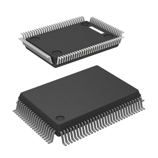


 工商网监
湘ICP备2023018690号
工商网监
湘ICP备2023018690号

